Following on from my review of the Keithley 2110, I tamper with the tamper-proof seal and open up the meter to see what was inside. While I am there I have a look at the build quality and the overall system architecture. Keithley have a long history of building quality test equipment and I thought it would be nice to see how the latest kit from Keithley stacks up to their past reputation.
The meter is easy to get apart and is built really well, nice solid construction and really very difficult to fault – apart from the really poor LCD display. Please see the video for the details as they unfold.
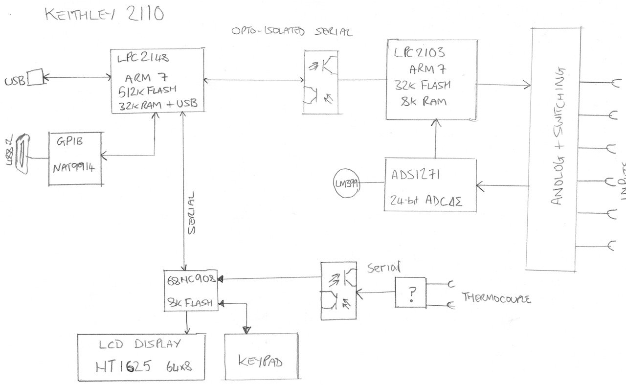
System Level Block Diagram
Catch you next time…
This content is published under the Attribution-Noncommercial-Share Alike 3.0 Unported license.
very fast teardown, i think you skipped the main part, the analog front-end, protections and adc
Some high res photos would be appreciated too.
thanks
Hi, I did not try to reverse engineer the front-end, there was far too much discrete there and there would have been a lot of probably not that useful guesswork. I did cover the main ADC and the RMS converter, of course you can probably get much of the detail from those data sheets. I mentioned and showed the front end protection too I thought, not in great detail but it was there. I could have gone into more detail I guess, I will do next time. Hi res photos are something I have not done much of in my tear downs, I probably could but time can be an issue for me. Thanks for the feedback.
Gerry
I was most interested in the adc layout, grounding, connections to digital circuitry, power supply distribution and so on and since you had some experience in these kind of circuitry i guess your insight would be much informative, in this teardown i didnt even get to see the back of the main board 🙂
thanks for your efforts and keep up the good work
and by the way still waiting for that p.s. firmware video 🙂
Hi Ali,
Yes fair point. When I looked at it, nothing remarkable stood out to me but of course that is because I probably have a good idea what to expect. I will make sure I go into more detail next time. Thanks for your comments. The PSU is still ongoing, I have not stopped, I just hit one of those points in the project where there is a lot to do with very little progress being made – watch this space..
Gerry
Hello George.
I know it’s been a few years since this teardown, but perhaps you written down or may remember what was the full partnumber of the MC68HC908 MCU on the front panel. The partnumer usually goes like MC68HC908XXYY where XX denotes family and YY Flash size.
I watched the video, focused on the front panel teardown, but I just couldn’t decipher it.
Thank you.