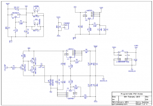
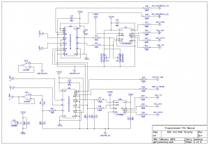
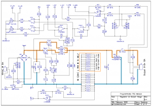
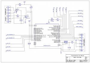
Here is the latest Revison 0.4 schematic which represents the power supply design as described in this blog and videos with the latest round of prototyping and testing.
The headline changes from last time are as follows: –
- I have added -Ve supply using a simple charge pump and a PWM drive from the micro controller.
- I have added a difference amplifier to correctly handle remote voltage sensing for both PSU voltage control and output voltage read back
- I have modified the design to use low-side current sensing instead of high-side current sensing. In doing so I have dropped the use of the high side current sense amp MAX4080 and made use of a spare op amp element instead. This saves a $3 part and replaces it with half of a $2 part
- Removed dedicated buffer amp previously added to drive the ADC, the new design removes the need for this because the voltage and current monitoring are better buffered now. This saves another $2 part.
- Moved to a faster micro controller PIC18F46K22 which has more memory, more PWM outputs and more I/O pins. No real reason apart from I needed a second PWM output. The firmware is pretty much compatible.
Here is a video overview of the design changes and latest prototype hardware and test setup as well as some basic tests showing load regulation and programmable voltage accuracy benchmarked against a calibrated HP 34401A bench meter.
NOTE: I used a different mic setup and the sound is really poppy and crappy! My apologies…..My dustbin now has a new microphone in it!
You can download the hand-drawn illustrations used in the video here: PSU Part 11 Illustrations
So I am working on the final PCB now, in Part 12 I should have a finished module….whoop whoop….Please do comment and like the videos if you find them interesting. Thank you for watching.
This content is published under the Attribution-Noncommercial-Share Alike 3.0 Unported license.


Hi, i’ve been following this very interesting project for some time now, and plan to build my own. Looking at the schematic for the ADC / DAC circuit, one question pops up. Why don’t the DAC and ADC share the same SPI-bus?
Best, Jonas
Hi Jonas,
That’s a good question. They do not share the same bus because of the way the two devices work. The ADC is being used in auto sample mode, that is, the chip samples continuously and each time it completes a sample it signifies its readiness by setting the data line low. This in its self is not that SPI friendly so I poll for that event by lowering its CS and checking the state of that line. When I sense there is data, I read in the remaining 31 bits. The protocol the chip uses to do this is not SPI peripheral friendly so it’s all done by the micro bit-banging as needed. The sample rate is only about 6.7 per second so performance is not an issue. The DAC on the other hand is using the SPI peripheral on the micro, this is done because of speed mainly, the DAC’s values are being continuously written at a rate of a thousand values per second on a timed interrupt, this is because I am modulating the DAC’s output to expand its resolution to and effective 18-bits, and this is not feasible to do by bit-banging.
Once I finish the design I was thinking about getting a batch of PCB’s made if there is enough interest – that might save you a bunch of work if you want to build one yourself.
Gerry
Hi Gerry,
Ahh of course – thanks for the explanation. Instead of bit-banging, why don’t you use the other SPI bus (pins 2, 38 & 39), available on the (now bigger) PIC? I’m definitely interested in a couple of pcb’s, so count me in!
/Jonas
Hi Jonus,
another good question. Its because I was being lazy 🙂 the firmware is basically working and I could not see a need to change it, I have plenty of spare pins. However, going back to the way the ADC works, it asserts a low (or high, I can;t remember off the top of my head) when it has a sample ready, so by lowering CS and looking at the data pin, this tells you if the data from the ADC is ready, and it also tells you if you should read the rest of the data. If you do, another sample is started after the read, if you don’t then the current sample completes, a false read actually re-starts a new sample abandoning the current one. The problem with using the SPI peripheral is it does not understand this so I could not get it to work. There is also an issue with the ADC providing the clock, I can’t really remember now. I first connected the ADC and did use the SPI peripheral but had all sorts of trouble reading it, in the end bit-banging won out.
Gerry
Hi again Gerry,
have you totally given up on the pre-regulation circuit? I can see the AC_SENSE signal is still wired to the uC, but am I missing something?
/Jonas
Hi Jonas,
Yes I have decided to drop this for now. The original concept was to use simple PWM control and the smoothing caps as the low-pass filter. I was not happy that I could make it responsive enough to work through the micro so making it work would require a controller chip of some sort. To go to that trouble it really ought to be a proper buck regulator so I at that point I decided to remove it from the design so I can focus on getting it finished. I do plan to re-visit this, you will see in the next post how and why.
Gerry
Hello.
Your project looks great. What the specifications of this laboratory power supply unit? When we can to expect… i don’t know, maybe pre-final version of it?
Thanks.
Hi Kreker,
The specifications are variable, depending on the builders needs. The design is based on an idea of being modular. Project so far focuses on a module which would represent a single channel. If you want a two channel PSU you would make it out of two modules. The module can be configured for different ranges (broadly set out in this article: http://gerrysweeney.com/fully-programmable-modular-bench-power-supply-part-9/ ), the module can be configured with just a few resistor changes and a couple of solder jumpers. In terms of specifications in accuracy and load regulation etc i am aiming to get this as good as my Agilent E3631A triple output PSU.
The next part (12) should have the final version of the module, I am just waiting for the PCB’s from manufacturing.
Thanks for following the project.
Gerry
Hi Gerry,
I must say, this particular thread is surely the most up-to-date PSU project around. I’ve been searching for a nice dual-tracking project for a few weeks and have been reading/re-reading this one for few days now.
I have some familiarity with Microchip PICs and spend a lot of my hobby time using the dsP33xx for motor control … and I have very limited analog experience. So my question is about the DAC implementation on a separate chip vs an on-PIC PWM/Low Pass Filter implementation using i.e 16-bit dsPIC30Fxx. Would that be more prone to i.e board noise, control variation, etc?
Last question(s) … is the GUI you’re using working through the PICs ICSP with MPLAB? If so, what is the software? Just curious.
Thanks for the time and effort you are putting in on this project.
Mike
Hi Mike,
Thanks for your interest in the project. As far as I am aware, even with a dsPIC, my options for a DAC are still limited to digitisation using PWM of one sort or another, although higher resolution might be gettable from using SDM or other Delta-Sigma variation, in which case a dsPIC might be useful – but my question would be around error introduced as a result of software processing. I am pretty sure that PWM can be made with improved DNL/INL with the right circuitry, although I have not tried it yet, I would need to build up a circuit and try it out. Because the way the timers work in a PIC/dsPIC and work directly from the clock/4 (normally) I would expect there to be very low jitter and should be able to get good accuracy. I would expect the output of the PWM would need to switch a high accuracy/stability voltage reference into the low pass filter, and a precision active low-pass filter may well be needed and I expect the type of caps would also be of importance for stability. Its an experiment to be done 🙂
The GUI is written in C++ using Qt, its working through the serial interface on the PSU board which is opto-isolated, I am using an el-cheapo USB to Serial/TTL adaptor to connect to my iMAc.
Gerry
Nothing personal, but i think that you did chose wrong way. Need to avoid the parts, which cost like 50$ per one (have a bad ratio of price and quality), because 5-10$ per some important part of device with good quality / precision it is not so much. For example, so much better will use a) LT1963A , FLT3015 instead of LM317; b) bipolar power amplifier instead LM358, if it required; c) digital DS1821 instead transistor, and etc.
There are many branded power supplies, but only a few of them have needed features. And the price per this devices aren’t so small.
But it’s only mine opinion, because you are engineer and have much more expirience in practice.
It does not matter if you disagreed with my words, this power supply is clearly better than the others are. More difficult, but better. Moreover, if it can provide 40-50V and 4-5 A – it’s my choice. (Please, can it be true? :D) And maybe i can to change some parts of schematic by myself or with your help.
I’m poor student and I can build this lab power supply, but not immediately. And i can do some small donation.
2) What you thinking about feature when one of type of protection was TURNED ON and PSU off its output to the load, which plugged to power supply?
Like at this schematic: http://tinypic.com/r/oqya2r/6
3) [crossed out] You can get a non-profit license of DipTrace with 1000 pins limit if you’ll using it for non-commercial purposes. Just contact with the developers. Or we can to think about it, please contact me via e-mail. [/crossed out] Looks like you own Diptrace already. 🙂
Thanks for reading and sorry if I did\said something wrong. Waiting for true final version.
Hi Kreker,
I am not sure I understand your rationale, I am using LM317’s because they are not only cheap but for what they are being used for they are also perfectly adequate for the job, there is little point in putting a high-quality regulator in to generate a supply for a circuit that has a relatively high CMR by design. LM317’s are really quite good for what they are – they are cheap mostly because they are produced in such high volume and are ubiquitous in may areas of electronics. Parts and their costs are an important thing to focus on in electronics design, a good design should consider economics as well as other attributes. using a DS1821 is really no advantage over an MCP9700, if I am within a degree C thats good enough, I only need to spin the fan up if the heat sink is getting too hot or shut down the output if its way too hot. A DS1821 costs upwards of $2 each, an MCP9700 costs 30$, the DS1821 is really not needed and adds complexity for no reason, actually one could argue it would degrade the design because of the additional radiated noise from the digital communication with the device. Not sure I understand your question about protection – being a constant current regulator, output protection is built in. I have added some diode protection and a fuse to prevent damage from reverse input conditions.
I would correct you on one point though – I am not an engineer, not a professional one at least. I have messed around with electronics for about 30 years in one form or another but hardly ever in a formal or professional capacity. No university engineering degree here – I am self taught through both experimentation and have been fortunate enough to share knowledge with a few good people who have similar interests over the years – I am known for my persistence 🙂 drawing inspiration and being driven from a deep-rooted interest in the subject with a strong desire to create. Does that make me an engineer – not sure it does…
Gerry
On being an engineer: In my opinion you are an engineer if and when you act as an engineer. That is, you apply scientific knowledge and practices to solve real-world problems.
The university degree is superfluous. No degree ever designed a circuit and I’ve met a number of folks with degrees that couldn’t design their way out of a three sided box.
Professional is another matter. A professional is someone who does the activity to generate a source of income. Getting paid makes one no smarter (nor less smart) than an amateur.
Thanks for your observations. Gerry
Hi again.
I have some problems with English language, so i’m sorry for possible misunderstanding.
I have another interesting schematic implementation.
http://tinypic.com/r/psi7s/6
http://tinypic.com/r/2qwo3ux/6
This is switcher of transformer windings, which was used in PSU HY-3010. It shall help to reduce the overload power, which released at transistors. Do not pay attention to some errors, it’s just a sample. Whether will be such feature a useful in your PSU?
Hi Kreker,
I did consider this approach, this is very common and done in many power supplies. For this project, I wanted to keep the design so it would work with more off-the-shelf transformers, ideally a single secondary winding. In the early incarnations I included a pre-regulator using a bucket charge pump approach but later removed it for reasons explained in the article series. However, I am very definitely going to re-visit this but I decided to continue developing the supply without the pre-regulatior for now. When I do re-visit, I am currently favouring a buck switcher, which is efficient and pretty simple to implement (famous last words). Thanks for posting the links.
Gerry
Hi gerry,
Nice project by the way, this is my first look of our project, but i have a question (sorry if you have talk about in another video), the question is:
Why you don’t use a floating ground to generate a clear an stable reference to 0V, you eliminate the offset error’s, generate by the parasitic resistance of the return circuit ( caused by the 8 Amps max current)
Best regards.
Hi dsantos,
One of the original design goals was to power the entire circuit from a single transformer winding to keep the cost low by being able to use off the shelf transformers, one winding per channel. Your suggestion makes sense, perhaps I should have used an isolated DC/DC converter. Anyway, I have a working scheme now although it certainly took some effort to make it work.
Gerry
Hi Gerry,
Just read thru your blog and watched the videos – Amazing!. Was wondering if you have completed the project and have a final schematic and pictures of it in action. I am only a beginner in electronics and was thinking of building a PSU as a project to learn more. I think once I have made a multi fixed voltage PSU of say 9v 5v & 3.3v I might give something like this a go.
Cheers and much appreciated for your detailed explanations.
Hi Damien,
I got to Part 14 where is basically complete and you can see it working, the schematic is good for that range. It should easily scale across to the 0-40v 0-2A range too, I have just not get around to it yet 🙁
Gerry
Hi Gerry,
i am trying to make CC-CV (0-24VDC- 0-30AmpDC) Power Supply using LM723 and 2N3055 series pass transistors only, but i stuck in CC mode, can u please help me.