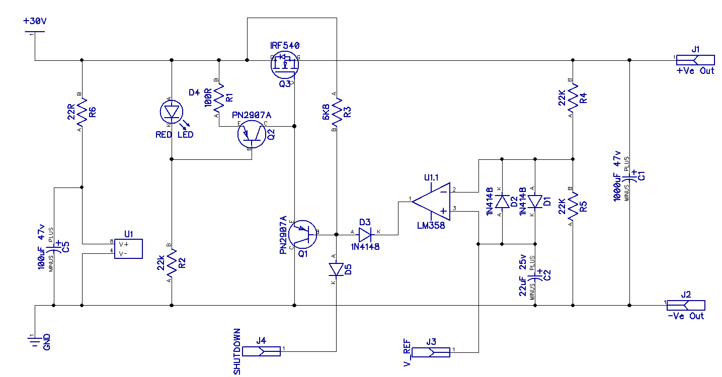
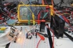
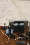
After a fair amount of playing about, measuring and trying things I finally arrived at a working design. I am happy I have what I think is a good starting point of rest of the project. I have something that is working and feels much more stable under a varying capitative and resistive loads, I have a high degree of confidence that I am now on the right track. Having resolved the issues with stability I have now added a current shunt, high-side current sense amp and current error amp for current regulation, I have also added a couple of amps in comparator mode to sense the regulation state to show if the regulator is in constant volts or constant current mode or out of regulation all together.
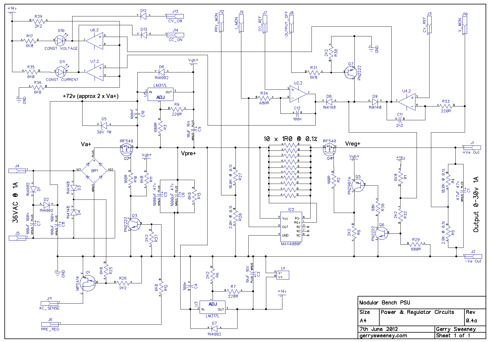
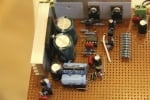
To sense current I have used a high-side current sense amp type MAX4080F, this is a really nice single chip solution designed for the exact purpose, it has a wide supply range and the “F” version has a x5 gain factor. Using a high-side current sense amp means that I do not need to sense in the ground return path which in turns helps keep things simple. The MAX4080F reads the voltage dropped across the current shunt which is made up of 10 x 1R resistors in parallel. The voltage read is multiplied by 5 and delivered to the output pin. In this configuration a load of 0-5A gives me a voltage output of 0-2.5v which is fed back to the current error amp limiting current to what has been set on the CC_REF input.
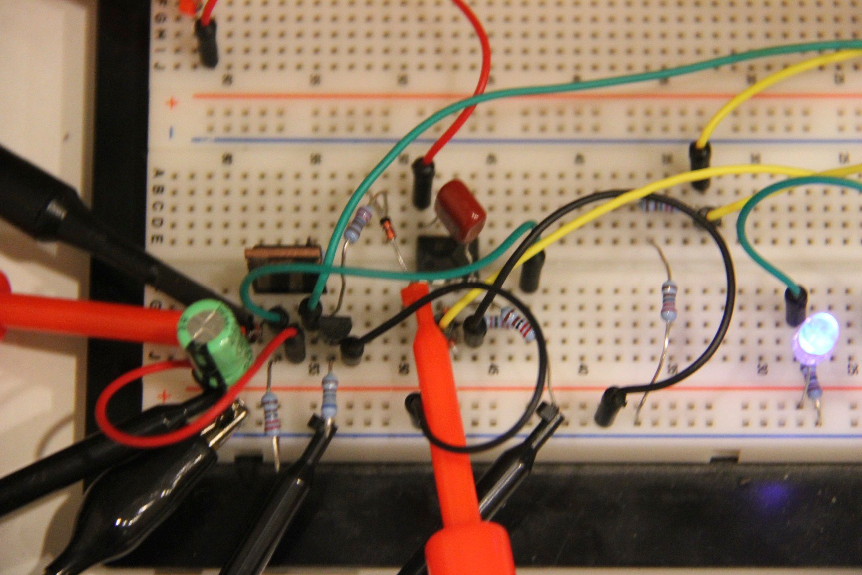
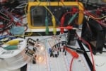
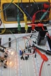
Here is a quick video taken to show the constant current limiter kick in as a filament lamp warms up and current demand drops. Turn the PSU output on and the cold lamp draws current beyond the limit set (indicated by the red LED), but as the lamp warms up and draws less current the PSU transitions from CC mode to CV mode smoothly.
In Part 3 I mentioned the idea of having a very stable low-power full voltage range regulator, this is what I created around Q5 and Q6, with R8 acting as its load. The IRF540 Q4 is then simply acting as a voltage follower which scales up the power handling, its source simply follows the voltage on the collector of Q5. This configuration works really well and is much more stable (more on that in a second), but its not perfect. I am not entirely convinced about the use of a FET as the final pass device any more. Its easy to drive because of the low drive current needed, but being a linear regulator circuit the output FET never does the one thing that its really good at which is being turn hard on, so despite having a positive grid bias supply that will allow this, its never used. The FET device is perfect for the pre-regulator switch (Q2) so I don’t need to change that but it would seem like there is an opportunity to simplify this circuitry further in the final output and driver section, so this is not yet a finished design, but its certainly a workable one. The decision may well come down to the bill of materials in the production, if we are using the FET for the pre-regulator, then we may as well use the same device as the pass transistor – we shall see….
For now I am not expecting to use the pre-regulator, it is in effect wired out by being switched on by default, If you were to build this circuit as as and do not wan’t pre-regulation (as would be the case in the 0-6v configuration) you would simply exclude Q2, Q3 and their associated bias resistors and put a link on the board between the drain and source pins where Q2 would have been. The pre-regulator will be introduced later and is specifically required to lower the overall heat dissapation of the regulator circuit under certain load conditions. The pre-regulator switching control will be done by the micro processor in the main but I do need to add some direct analogue feedback mechanism to ensure the regulators dynamic response is not impacted by any software or hardware latency the micro controller would introduce in this setup. Basically the idea is to sense any significant change (ac coupled) on the control point at the junction of D8 and D9 and if detected turn the pre-regulator hard on for a set period of time, lets say 250ms or so which will ensure full power is immediatly available to the drain of Q4 which will regulate as required. During this forced on time, Q4 will dissipate all of the heat generated by the power dropped across the regulator. Because of this forced on time, the micro controller will have time to sense the large amount of power being dissipated by Q4 by sensing the voltage differential between PRV_MON, I_MON and V_MON and will start driving PRE_REG to take over, in effect this is a lazy pre-regulation control that will only kick in once the load has stabilised, the micro controller will slowly wind down the power delivered into the resevour caps by switching the 100Hz drive from the bridge rectifier on the rising and falling slope of the half cycle, keeping a reasonable differential across Q4 for the given load. The pre-regulator control switching will be synchronised to the line frequency which will be sensed via the AC_SENSE signal.
Back to the regulator stability topic, I have removed all the capitative loading around the driver and output circuit and instead reduced the bandwidth of the control loop by including frequency-dependnat negative feedback on both the voltage and current error amps. The aim was to significantly lower the gain of the loop above the point where the feedback becomes positive and the servo action becomes unstable. The simple first order filtering built around R33/C11 and R34/C12 provides a very stable control loop in this configuration. DC conditions remain in tact but as the frequency rises in the circuit, then the negative feedback starts to kick in via C11 and C12 lowering the gain in the feedback loop. The filtering could be improved and there is definitly some improvements I need to make at very low output voltages (0-50mv). The basic regulator circuit I have ended up with is pretty classic and has been done many times before so there is nothing new, but for me what I have achieved is creating a circuit from the ground up and getting my own understanding up to a level that allows me to properly comprehend the behaviour and problems that can occur with such a circuit and some basic ideas on how one would tackle the problems when they do arise.
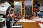
The regulator in the configuration shown means there is a x10 voltage gain, so for 0-3v in I get 0-30v out, and for current limiting, for 0-500mV in I get a 0-1A current limit. Doing some basic testing I was able to drive a load well above the rated power of 30W (almost 50 watts) without a problem and with good load regulation. The regulator tracks very accurately according to my Fluke 289 and Agilent 34401A into both load and no load conditions. I was able to short the output out while it was driving into a half load, full load and no load with no damage or noise problems – the current limiting works nicely. I have yet to do any testing around dynamic response, I don’t have a programmable DC load so I need to work up a simple test rig to do this which I will leave for another article.
I have based the entire design on a single rail power supply for the op amps, using single supply op amps type LM358, these are common, low cost devices. I have tried using LT1013 precision op amps in this circuit but there is not any improvement over the LM358’s, primarily because the circuit remains accurate because of the control loop that ensures this, so precision op amps are not needed.
As a final check, I was measuring the output noise on a scope which was looking pretty disappointing, I was getting 25-60mv of white noise and some very minor high frequency ringing, I think the latter could well have been scope leads etc. Slugging the output with a big electrolytic cap helped reduce the noise but it was still present. Having tried a few things I suddenly realised that my test setup was flawed in relation to noise testing. I was using the 0-6V range on my Agilent E3631A to derive my CV_REF control voltage which is bad. Firstly the Agilent PSU generates some noise, about 2-3mv worth of it and secondly, my regulator circuit is a x10 amplifier so i was amplifying whatever noise the E3631A was generating by a factor of ten. I tried the same test but driving the CV_REV signal from a 1.5v AA battery cell and low and behold the noise figures plummeted to below 2mv on the output into a load at 16v – lovely. I have not carried out tests of any substance yet but the early results are very encouraging.
So I now have a working regulator, what next? In Part 5 I am going to set the regulator aside for a while and turn my attention to the digital control circuit. I am going to use a micro controller with a DAC and ADC to try to create stable and accurate control reference voltages to drive the regulators CV and CC reference inputs as well as relatively accurate and high resolution metering to measure the output volts, current delivered and pre-regulator voltages. I want to achieve good accuracy for both reference voltage generation as well as metering but plan to try various configurations, DAC/ADC’s and software approaches to see see what can be achieved at a sensible component price point.