The Good, the Bad and the Ugly – Schematic and PCB Software

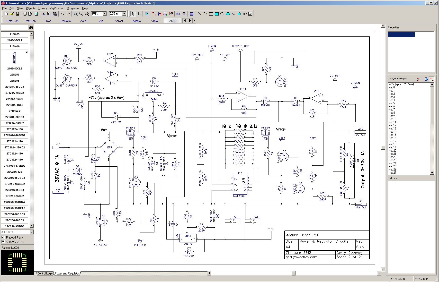
I have recently been using Diptrace for schematic capture and have just hit the 300 pin limit so I am looking at my options including alternative packages. Why am I looking at options? Having read numerous forums and reviews, based on other peoples experience it would appear that Diptrace is an improvement over Eagle and other low end solutions, I have tried Eagle In the past and I would have to agree, but Diptrace far from perfect, in fact its so poor in some areas I am now thinking about sinking time into evaluating other applications. Perhaps the EDA/CAD world has lower expectations that I do but even Diptrace which would appear to be the more intuitive of the bunch, the user interface, and more specifically the usability really sucks, it could be Sooooooooo much better.

Diptrace Screenshot

First of all, Mac OSX support. They claim it runs on Windows and OSX which is true. But on OSX its actually running the Windows version of the software under a windows emulator called WINE. Worse than that, WINE runs under Quarts X11 which is yet another layer of abstraction before it hits the actual screen. Trust me, the thing is crappy, actually bad enough that I want to use it in Windows instead, which is tearing me away from my beloved MAC. Integration into the Mac is non-existent, files and folder structures are ten folders deep as the WINE emulator creates a Windows-like folder structure. Novram should be ashamed of their claims of OSX support, its really terrible. The software also randomly hangs which causes work to be lost, the UI is slow and cumbersome and the keyboard shortcuts sometimes stop working so you are restricted to right-mouse context menus for cut/copy/paste delete until they magically come back from time to time. So if you are going to use Diptrace, use it on Windows not a MAC. If you have a Mac, install Oracle’s virtual box, run a copy of Windows 7 and use it as a native Windows app (I am going to give DipTrace one more try under Windows to see how I go).

In terms of the hanging, they have actually added a menu option called “Recover Schematic” which mostly gets back your last changes. They have added this at some point I imagine to deal with the fact that the software is buggy and can crash/hang. It would have been better to improve the software so it never needed an option to “recover” anything…

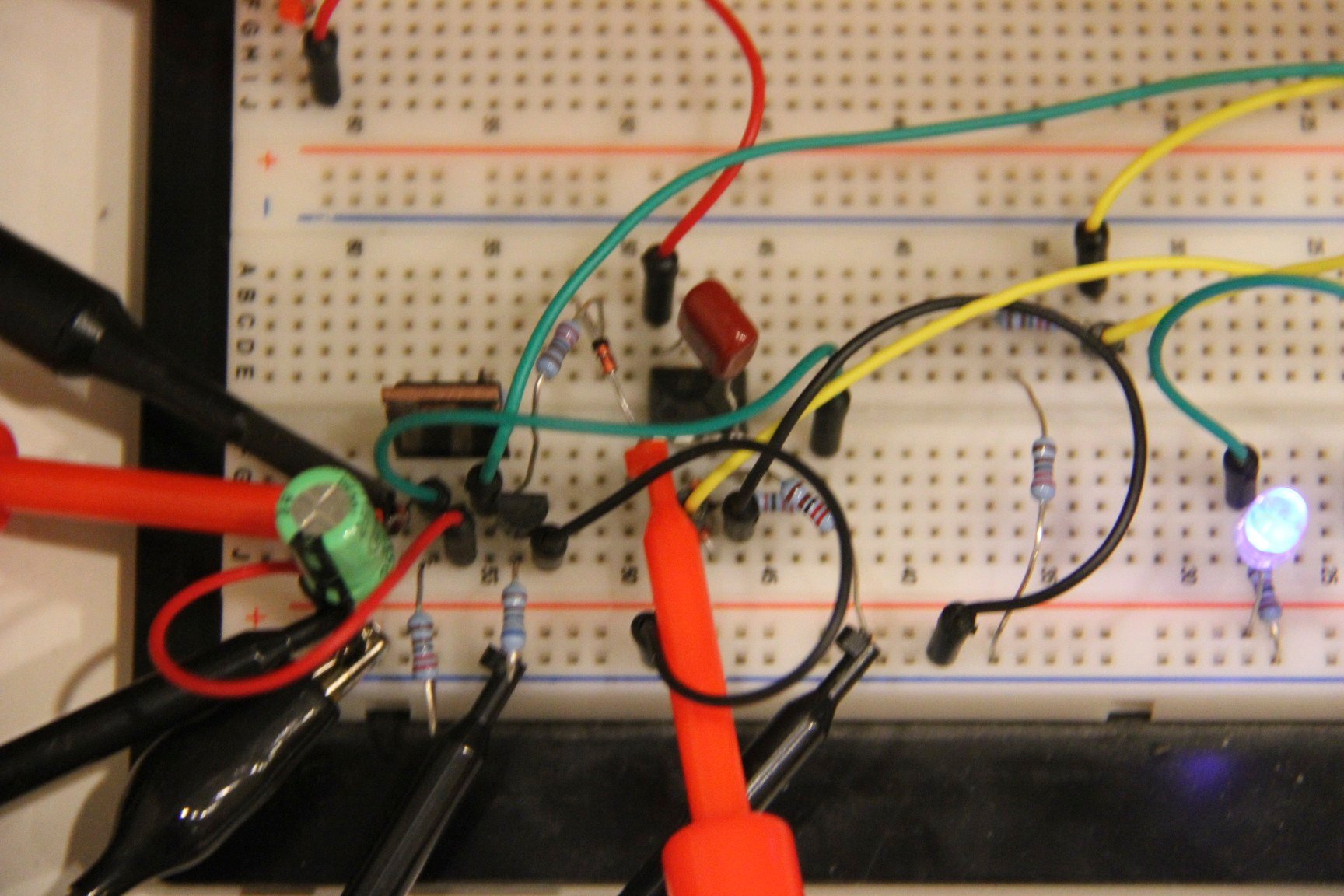
Now onto the features of software. I have to say at this point, I don’t much like CAD software, it all seems to have “its own way” of working, seemingly much of this is a hangover from Autocad which was made before a mouse was even commonplace, so lots of strange keyboard shortcuts etc. DT reacts strangely to the mouse mostly so while people seem to think its intuitive I can only imagine other packages must really be bad. If you are used to using Windows or Mac UI’s and you have not had any CAD experience then DT will feel alien and it has a long learning curve to get you past that. I have used it (schematic capture) to create a project and it does work once you get to understand its oddities. Being a software guy I know how easy it would be to make considerable usability improvements with little effort which makes it all the more frustrating – I first came across DT about four years ago and I have to say its not really moved on from then, and that is even more frustrating. The lack of development progress and the poor usability does not say a great deal for Novram.

Here are my top 10 specific bugbears…

1. No control over what component elements get displayed or printed. For example, on screen I see the pin names (B,C E) for the Discrete/NPN item, or A/B on the RES item, I don’t want to see them but I can’t turn them off without also turning off the pin numbers for IC parts which I do want to see. Any electronics engineer knows which pin is the emitter of a transistor, displaying E is ridiculous. Control of this should be a properly of the part not a global view property, although you might want that too.

2. Netports appear in the BOM, I have to manually remove them from the BOM after the export to a file, there would appear to be no way to control this. It would appear that NetPorts are just another 1-pin component which is why this happens, perhaps a simple attribute on the component property called “Exclude from BOM” might help.

3. The sheet connectors are stupid, Place one and it defaults to place a bus, try to place a wire and it sort of works but the wire does not align correctly. Strange behaviour….So don’t use “Sheet Connectors” to connect your circuits across sheets, use NetPorts instead – obvious really – NOT!

4. The library selectors on the toolbar are a little odd, the names are untidy, just a lack of attention to detail. Why call something that will be displayed in the UI Con_Sch, thats the sort of name you would expect to see in code, not presented to a user. Once you select a library you get the components down the left-hand side to select from – scroll up and down this enough selecting items (as you do when you are finding your way around the libraries) and you will get it to hang the whole program. Clicking an item puts you into place mode meaning you have to press escape if you were just browsing. Right click also cancels it but you also get a right click context menu. The little drop down on the library bar drops down a scroll bar so you can scroll through the library buttons – this compensates for a poor UI design making it even more unusual. The software could do with a decent library browser and some better organisation for the actual libraries. Trying to manage parts, copying between libraries etc, all very confusing and counter intuitive.

5. Create multiple sheets which is great, but then you want to change the oder of the sheets to more logically represent the flow of your project. Tough, you just can’t do that – at least I have not found a way so far.

6. A “Save All” button would be nice….instead of having to go to each sheet and save it separately.

7. There is a need for much better schematic annotation. Single line text is really not good enough. Ideally multi-line post-it style boxes would be good.

8. When drawing a schematic with a large IC you need to be able to re-organise the pins on the component to suit the schematic you are drawing – there is no option to do this apart from create your own library, copy the part into it and re-organise it for your specific schematic….rubbish….

9. Ever hear of smooth drawing using anti-alias? No! – neither have Novram – you could argue this is not needed but I would say if you are going to stare the the thing for hours on end you want it to be easy/soft on the eye – you could argue that it will make things slower – all true but I would still like to see my creation looking nicer.

10. Float the mouse over a connection and see the net highlight – nice – what about across sheets? Nothing doing, leaving you to manually check the net names to make sure your schematic has integrity across sheets. I thought computers were meant to make less work – not more (Microsoft, please take note of this point too..)

All in all it does work and its alright I suppose but after serious use I am left with a compelling desire to find an alternative – why is that, I don’t have the same feeling after using my e-mail program or my word processor. All of the pro’s seem to favour Altium designer http://www.altium.com/ but I can not bring myself to spend $3000+ for a piece of software that is really overkill for my limited use…I would love to evaluate it one day though – not sure Altium would want me to 🙂

I am about to try AutoTRAX DEX, you can find it here http://kov.com/. I bought this about four years ago and Oh-my-god, it was the most buggy and terrible piece of software I could ever imagine. It was cheap enough though that I did not loose any sleep over it when I just chalked it up to experience and uninstalled it. The author was defensive and it was pretty clear things were not going to get addressed and it was even more abundantly clear with the very regular, sometimes daily releases that there was absolutely no quality control, one new fix and another things broken etc, I gave up after a couple of weeks. At the time the guy developing it was focused on this next generation written in .NET and an all new design, this is now 4 years in the making and I recently had another go with it. On the back of a 20 minute play around I went and paid $49 and renewed the licence I already had.

I will evaluate AutoTRAX and write a detailed review with what I find. At a glance I can say is that a lot of attention to detail when it comes to look and feel, the schematics look really nice, they print well and the component libraries appear to be reasonably comprehensive. If it works well I think it could be a good contender for Diptrace, its a lot cheaper too, $99 for totally unlimited pins, layers etc…has 3D rendering and so on….

Fully Programmable Modular Bench Power Supply – Part 4

After a fair amount of playing about, measuring and trying things I finally arrived at a working design. I am happy I have what I think is a good starting point of rest of the project. I have something that is working and feels much more stable under a varying capitative and resistive loads, I have a high degree of confidence that I am now on the right track. Having resolved the issues with stability I have now added a current shunt, high-side current sense amp and current error amp for current regulation, I have also added a couple of amps in comparator mode to sense the regulation state to show if the regulator is in constant volts or constant current mode or out of regulation all together.

PSU Schematic Version 0.4a

To sense current I have used a high-side current sense amp type MAX4080F, this is a really nice single chip solution designed for the exact purpose, it has a wide supply range and the “F” version has a x5 gain factor. Using a high-side current sense amp means that I do not need to sense in the ground return path which in turns helps keep things simple. The MAX4080F reads the voltage dropped across the current shunt which is made up of 10 x 1R resistors in parallel. The voltage read is multiplied by 5 and delivered to the output pin. In this configuration a load of 0-5A gives me a voltage output of 0-2.5v which is fed back to the current error amp limiting current to what has been set on the CC_REF input.

Here is a quick video taken to show the constant current limiter kick in as a filament lamp warms up and current demand drops. Turn the PSU output on and the cold lamp draws current beyond the limit set (indicated by the red LED), but as the lamp warms up and draws less current the PSU transitions from CC mode to CV mode smoothly.

In Part 3 I mentioned the idea of having a very stable low-power full voltage range regulator, this is what I created around Q5 and Q6, with R8 acting as its load. The IRF540 Q4 is then simply acting as a voltage follower which scales up the power handling, its source simply follows the voltage on the collector of Q5. This configuration works really well and is much more stable (more on that in a second), but its not perfect. I am not entirely convinced about the use of a FET as the final pass device any more. Its easy to drive because of the low drive current needed, but being a linear regulator circuit the output FET never does the one thing that its really good at which is being turn hard on, so despite having a positive grid bias supply that will allow this, its never used. The FET device is perfect for the pre-regulator switch (Q2) so I don’t need to change that but it would seem like there is an opportunity to simplify this circuitry further in the final output and driver section, so this is not yet a finished design, but its certainly a workable one. The decision may well come down to the bill of materials in the production, if we are using the FET for the pre-regulator, then we may as well use the same device as the pass transistor – we shall see….

For now I am not expecting to use the pre-regulator, it is in effect wired out by being switched on by default, If you were to build this circuit as as and do not wan’t pre-regulation (as would be the case in the 0-6v configuration) you would simply exclude Q2, Q3 and their associated bias resistors and put a link on the board between the drain and source pins where Q2 would have been. The pre-regulator will be introduced later and is specifically required to lower the overall heat dissapation of the regulator circuit under certain load conditions. The pre-regulator switching control will be done by the micro processor in the main but I do need to add some direct analogue feedback mechanism to ensure the regulators dynamic response is not impacted by any software or hardware latency the micro controller would introduce in this setup. Basically the idea is to sense any significant change (ac coupled) on the control point at the junction of D8 and D9 and if detected turn the pre-regulator hard on for a set period of time, lets say 250ms or so which will ensure full power is immediatly available to the drain of Q4 which will regulate as required. During this forced on time, Q4 will dissipate all of the heat generated by the power dropped across the regulator. Because of this forced on time, the micro controller will have time to sense the large amount of power being dissipated by Q4 by sensing the voltage differential between PRV_MON, I_MON and V_MON and will start driving PRE_REG to take over, in effect this is a lazy pre-regulation control that will only kick in once the load has stabilised, the micro controller will slowly wind down the power delivered into the resevour caps by switching the 100Hz drive from the bridge rectifier on the rising and falling slope of the half cycle, keeping a reasonable differential across Q4 for the given load. The pre-regulator control switching will be synchronised to the line frequency which will be sensed via the AC_SENSE signal.

   
Average rating  1 2 3 4 5fYou must login to vote
IMG_5173.jpg
IMG_5176.jpg
IMG_5178.jpg
IMG_5180.jpg
IMG_5181.jpg
IMG_5182.jpg
IMG_5146.jpg
IMG_5147.jpg
IMG_5148.jpg
IMG_5149.jpg
IMG_5151.jpg
IMG_5153.jpg
IMG_5159.jpg
IMG_5161.jpg
IMG_5170.jpg
IMG_5171.jpg
IMG_5172.jpg
IMG_5173.jpg
IMG_5176.jpg
IMG_5178.jpg
IMG_5180.jpg
IMG_5181.jpg
IMG_5182.jpg
IMG_5146.jpg
IMG_5147.jpg
IMG_5148.jpg
IMG_5149.jpg
IMG_5151.jpg
IMG_5153.jpg
 

Back to the regulator stability topic, I have removed all the capitative loading around the driver and output circuit and instead reduced the bandwidth of the control loop by including frequency-dependnat negative feedback on both the voltage and current error amps. The aim was to significantly lower the gain of the loop above the point where the feedback becomes positive and the servo action becomes unstable. The simple first order filtering built around R33/C11 and R34/C12 provides a very stable control loop in this configuration. DC conditions remain in tact but as the frequency rises in the circuit, then the negative feedback starts to kick in via C11 and C12 lowering the gain in the feedback loop. The filtering could be improved and there is definitly some improvements I need to make at very low output voltages (0-50mv). The basic regulator circuit I have ended up with is pretty classic and has been done many times before so there is nothing new, but for me what I have achieved is creating a circuit from the ground up and getting my own understanding up to a level that allows me to properly comprehend the behaviour and problems that can occur with such a circuit and some basic ideas on how one would tackle the problems when they do arise.

The regulator in the configuration shown means there is a x10 voltage gain, so for 0-3v in I get 0-30v out, and for current limiting, for 0-500mV in I get a 0-1A current limit. Doing some basic testing I was able to drive a load well above the rated power of 30W (almost 50 watts) without a problem and with good load regulation. The regulator tracks very accurately according to my Fluke 289 and Agilent 34401A into both load and no load conditions. I was able to short the output out while it was driving into a half load, full load and no load with no damage or noise problems – the current limiting works nicely. I have yet to do any testing around dynamic response, I don’t have a programmable DC load so I need to work up a simple test rig to do this which I will leave for another article.

I have based the entire design on a single rail power supply for the op amps, using single supply op amps type LM358, these are common, low cost devices. I have tried using LT1013 precision op amps in this circuit but there is not any improvement over the LM358’s, primarily because the circuit remains accurate because of the control loop that ensures this, so precision op amps are not needed.

As a final check, I was measuring the output noise on a scope which was looking pretty disappointing, I was getting 25-60mv of white noise and some very minor high frequency ringing, I think the latter could well have been scope leads etc. Slugging the output with a big electrolytic cap helped reduce the noise but it was still present. Having tried a few things I suddenly realised that my test setup was flawed in relation to noise testing. I was using the 0-6V range on my Agilent E3631A to derive my CV_REF control voltage which is bad. Firstly the Agilent PSU generates some noise, about 2-3mv worth of it and secondly, my regulator circuit is a x10 amplifier so i was amplifying whatever noise the E3631A was generating by a factor of ten. I tried the same test but driving the CV_REV signal from a 1.5v AA battery cell and low and behold the noise figures plummeted to below 2mv on the output into a load at 16v – lovely. I have not carried out tests of any substance yet but the early results are very encouraging.

So I now have a working regulator, what next? In Part 5 I am going to set the regulator aside for a while and turn my attention to the digital control circuit. I am going to use a micro controller with a DAC and ADC to try to create stable and accurate control reference voltages to drive the regulators CV and CC reference inputs as well as relatively accurate and high resolution metering to measure the output volts, current delivered and pre-regulator voltages. I want to achieve good accuracy for both reference voltage generation as well as metering but plan to try various configurations, DAC/ADC’s and software approaches to see see what can be achieved at a sensible component price point.

Fully Programmable Modular Bench Power Supply – Part 3

Previously in Part 2 I created a simple regulator circuit using a pass device and an op-amp, I was basically putting the well understood theory of this kind of circuit into a practical circuit and verifying my own basic understanding. Apart from no-load DC conditions which were fine and dandy, any sort of even moderate resistive or capacitive load drove the circuit into wild instability, clearly the breadboard its self, thin connecting wires and long component leads as well as a lack of any star earthling were all going to contribute to this, so it was time to refine the circuit a bit and build it on a more sturdy vero board with some attention to layout, earthing and current handling. Here is the circuit I built: –

PSU Schematic Version 0.1

The initial prototype is a throw-away, that means I build it on vero (strip) board, use low/no cost components, cheap sockets for the IC’s I want to re-use and as many components as possible from the junk bin – when I am done with my testing I strip anything worth keeping for the next project and throw it in the bin – the point is, don’t expect it to be pretty…..

PSU Throw Away 0.2
PSU Throw Away 0.2

The significant change was adding gain to the circuit which is critical if I am to get the desired output range of 0-30 volts. The gain is obtained in Q1 which is in the classic emitter follower (if it was a NPN BPT) configuration. Having this configuration for the driver means I only need a swing of between 1 and 2v to get the full output swing of 0-30v. Needing a small voltage swing means I can run the op-amp at 14v. The driver and output is acting as a voltage amplifier which is what FET’s are good at doing. The diode D3 is ensuring that the op amp is running in class A in the required range driving into R8 which is its load. By doing this we eliminate any potential crossover distortion the op amp might exhibit because of its internal center point.

The op-amp U1.1 is doing the error correction. The driver FET (Q1) is inverting, which means the negative feedback from the output of the regulator is actually fed into the positive input of the op amp, this is a different configuration to the first design where the driver was a current amplifier and non-inverting.

One interesting addition is the Vgb+ supply voltage. You will see that I have included pre-regulator pass device (Q2), the idea here being when there is a large amount of power being dissipated across Q3 the micro controller can detect this and drive Q3 which in conjunction with C5 and C6 will act as a bucket style pre-regulator. Because Q3 is acting purely as a switch we need it to be both very fast and very low on resistance and one of the things a power FET does very well is have very low on resistance. However, in order to get this low on resistance, you need to drive the FET’s gate pin at approximately +5v above the source pin. That means if you have 30v on the drain, and you want to see 30 volts on the source, then you need to drive the gate with +35 volts. Vgb+ is obtained by using a simple AC voltage doubler and a series regulator that’s referenced from +5, giving 5v above V+ regardless of input voltage.

So filled with high expectations I power up my new masterpiece for the first time and err, well not great. Unstable is an understatement, I had high frequency instability, low frequency instability and wildly different variations of the same with different loads. For the most part, a large electrolytic cap across the output brought it mostly under control, the high frequency stuff was largely killed off by placing C12 on the driver (Q1). Various loads across the range would yield different results and it was unpredictable and certainly not reliable in a way that I would be happy to power my next project from it!

So whats going on? why are these types of circuits so unstable? Well, I am sure there are very detailed scientific explanations but I don’t have anything like the knowledge to explain those; so in layman’s terms this is the best I can do. Under perfect DC conditions, the ideal circuit (which is how I tend to visualise electronic circuits) there is negative feedback and no phase shifts so you have a perfect DC Servo, so it locks the output to the input reference and as load is placed on the output the error amp drivers more or less to maintain the output at the input level – easy right? Unfortunately, all electronic components, wires, board layouts power sources and environments generate noise and have parasitic inductance and capacitance all of which can introduce phase shifts at different frequencies – this means that across a frequency spectrum our perfect theoretical circuit with its perfect negative feedback actually turns into positive feedback and your stable DC servo becomes an oscillator, your circuit can be stable at one frequency and totally unstable at another frequency and this can be occurring at the same time. Worst case you have numerous different stable and unstable conditions concurrently.

As I was measuring this behaviour I was observing a lot of fluctuation, things were varying in a random and unclean way, the analogue equivalent of a random number generator in software. To me the circuit felt very loose and reminded me a lot of those old fashioned black and white CRT TV’s I used to play with when I was a kid, The whole thing was powered by a big dropper resistor and change in the percentage of white/black proportion would significantly change the voltage levels in the TV’s electronics and this could be seen visually as instability as the picture would appear to breath and move around on the screen as things changes. Compare that to later solid state CRT TV’s where regulated power supplies were used, everything was much more stable visually.

I had managed to quieten the PSU down and drive into loads with good regulation and I achieved this by slugging the think with capacitance which has the effect of lowering the bandwidth of the circuit, which means the circuit has no, or substantially reduced gain at higher frequencies and any oscillations at those frequencies obviously go away. The problem with reducing bandwidth though is the impact on the dynamic response of the PSU under varying load conditions (more on that in a future article).

Types of capacitor also play a big part, for example I was only able to stabilise the high frequency issue using a 3n3 to 10n polyester cop, putting in the same value in multilayer ceramic did not work – that was yet another indicator that the circuit is simply too sensitive to instability – its loose.

My test conditions were done mainly under a 5-10 watt load at about 15v. I have attached some photos and some scope traces so you can see the sort of effects I was seeing.

   
Average rating  1 2 3 4 5fYou must login to vote
IMG_5135.jpg
IMG_5136.jpg
IMG_5137.jpg
IMG_5143.jpg
IMG_5144.jpg
IMG_5145.jpg
IMG_5121.jpg
IMG_5122.jpg
IMG_5123.jpg
IMG_5124.jpg
IMG_5125.jpg
IMG_5126.jpg
IMG_5127.jpg
IMG_5129.jpg
IMG_5133.jpg
IMG_5135.jpg
IMG_5136.jpg
IMG_5137.jpg
IMG_5143.jpg
IMG_5144.jpg
IMG_5145.jpg
IMG_5121.jpg
IMG_5122.jpg
IMG_5123.jpg
IMG_5124.jpg
IMG_5125.jpg
IMG_5126.jpg
 

In summary, despite having it quiet and stable with various test conditions I was left with the impression that the circuit felt wrong. At this point I am suspecting many things, the FET’s are very fast so they were a concern, the feedback loop is running at high power levels so effects of parasitic capacitance and inductance are very pronounced. My overall take away was I need to start again and just for a while I thought, maybe I should just use an off-the-shelf IC solution – but I felt like I was giving up to easy. I don’t have the skills and experience to design this scientifically so I have to approach this with a bit of trial and error and a lot of instinctive sauce. That desire to not give up got me thinking – and an idea came to me – what if I created a very low-power regulator which was highly stable at the desired voltage range and then scaled that up with a simple current amp – could I get better results?

In Part 4 I will share with you the great progress I made and a fully working regulator design.

Fully Programmable Modular Bench Power Supply – Part 2

Now the overall high level system design and parameters are set (see Part 1), its time to get down to some practical design. As I specifically do not want to use one of those “out-of-the-box” all in one regulator chips the first thing we need is a working linear voltage regulator that we can build upon. Using the prototyping breadboard I created the following circuit. The objective was to set up and verify the DC conditions for a basic regulator. Unlike a classic regulator circuit where there is typically a fixed reference and a variable resistor (POT) in the feedback loop, this regulator calls for something slightly different because our micro controller and appropriate DAC will generate an accurate reference voltage between 0 and a couple of volts, the exact value of which will be set by the user; the regulator circuit must track this reference voltage and set its DC output to a multiple of that reference.

The following schematic shows my initial 30 minute attempt at building such a regulator.

PSU Schematic Version 0.1

I should state at this point that the circuit is basic and is missing lots of things that one would expect to find. The purpose of this initial design was not to create a perfect regulator but was to setup a circuit to verify the basic DC conditions and theoretical practicality of the circuit.

The circuit is built around a FET pass device (type IRF540) which is the power workhorse. Unregulated power into the drain with the load placed on the source. The op-amp is configured as a simple error amplifier. The op-amp will move its output up or down (depending on the input state) in order to get its two inputs as close together as possible. Because the op amp drives the power device and the negative input of the op-amp is derived from the output that the power device we have a closed loop servo circuit and this is in essence what a typical regulator is made up of.

Because of the closed loop nature and the tight feedback loop, one of the biggest problems with these types of control circuits is stability. Each component and any introduced capacitive or inductive loading will create phase shifts (all components exhibit parasitic capacitance and inductance). Phase shifts will put the circuit into positive feedback at certain frequencies so there is a good possibility that such a circuit will become an oscillator at certain frequencies. As a consequence, a great deal of attention needs to be paid to this problem in the design which needs to ensure that it works reliably and remains stable within the scope and specs of the requirements. The more voltage and current range required the more difficult it is to tune the circuit to be stable of the range. Component choice, DC conditions, speed/bandwidth, gain, noise and PCB/Track layout all matter a lot here. It’s for this reason that many power supply designs avoid discrete solutions in favour of a one-chip solution. Discrete regulators are hard to make, and even harder to make reliable and stable and to be honest, most people cannot be bothered when there is a $2 off the shelf IC that will do the job most of the time. However, a professional grade programmable bench power supply needs something more than what these one chip solutions offer.

Considering the breadboard approach to building the above circuit (see photo) under moderate loads the regulator circuit was pretty stable, actually I was very surprised just how stable it was.

Birds Nest Construction

I thought I was on my way but very quickly realised I was actually on the wrong track. The reason why this design is stable is because it does not have much gain, in fact it has a gain of just 2. So put 2 volts into the V_REF input and get 4 volts out. The driver transistor Q1 is in effect a current amplifier in this configuration – the op-amp has to swing its output pretty much the range of the desired output. For low voltage requirements where you con comfortably run your entire circuit from a single supply this is a very good approach because of the inherent stability of the circuit. However, this design requires a regulated output of 0-30v which would require the unregulated input voltage after the rectifier and reservoir caps to be about 45 Vdc. Not many op amps can run at this level, and those that can are only just within range so we would be right on the edge of the spec for the device which does not make for a robust design and I personally don’t like components being pushed to their limits – it feels wrong, a bit like driving your car continuously in the red like, you can do it but not many people want their car to scream like that all the time.

In order to facilitate ease of use and the modular design I have set out to achieve, I want to create a regulator module that runs from a single AC power source, a single winding from the mains transformer. Many bench PSU’s (for example, like the Agilent E3631A I recently repaired) have multiple internal power supplies where the control circuitry is powered separately from the main power source. This makes it easier to design for higher regulated voltages and helps with things like noise immunity too but because of the design goals I have set it’s not an option for this design.

The design needs to take into account some system design constraints. No split supply for the op-amps, so we need to use single-supply capable devices. The op-amps and control circuitry need to run at a much lower voltage than the pass device and regulator output and the only way that is possible is by introducing voltage gain outside of any op amp. Voltage gain using an emitter follower (or equivalent approach) provides the level translation needed and lots of gain but that’s where the stability problems start.

In Part 3 I will describe the next evolution of the regulator circuit where I introduce gain and a considerable amount of instability and start to formulate a workable solution.