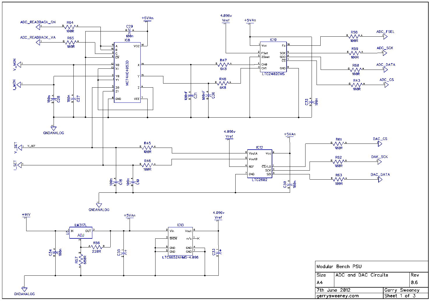
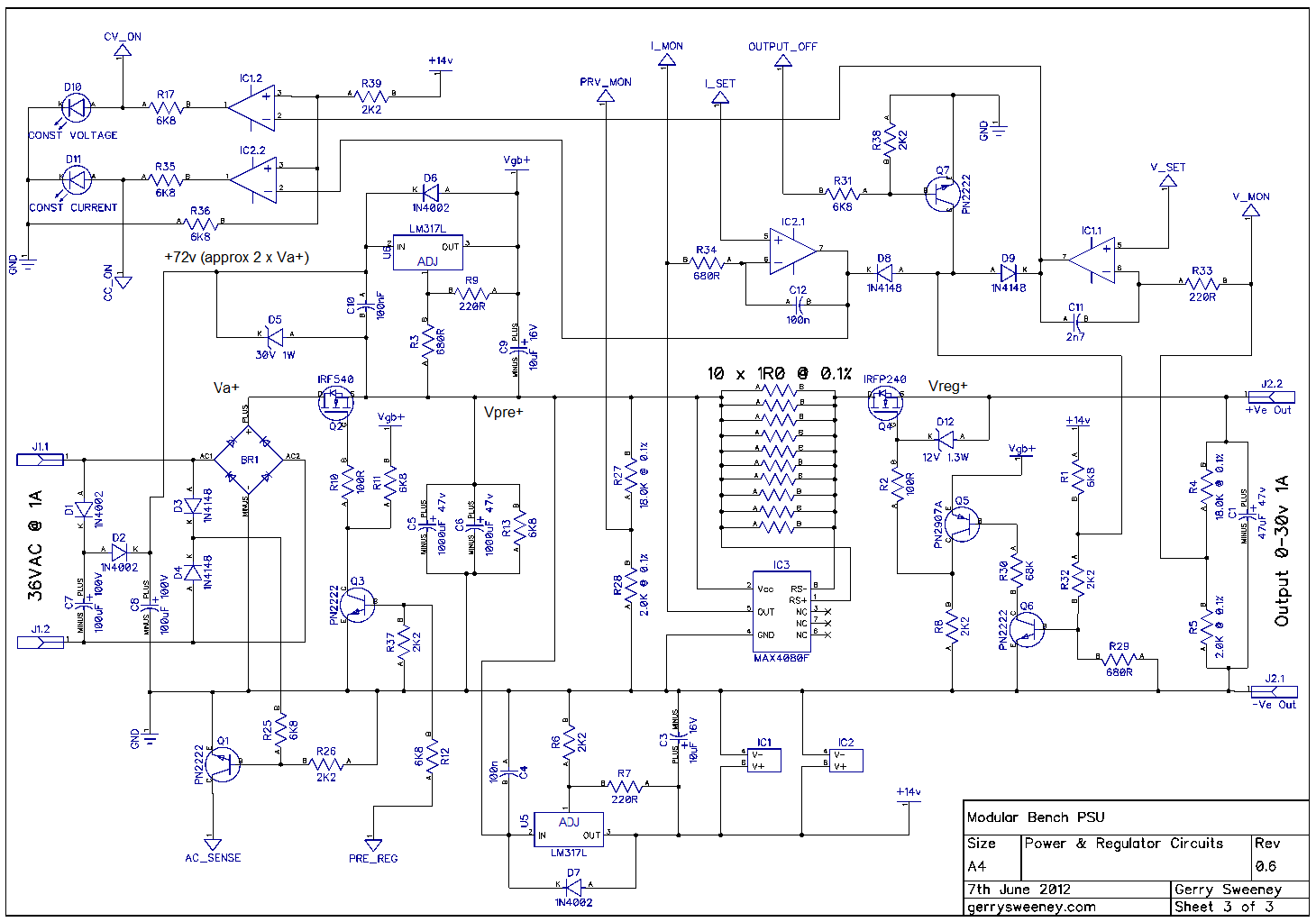
After a fairly disappointing start with the 12-bit DAC from Microchip I have chnaged the DAC to a 16-bit resolution part LTC2602 from Linear Technology. The goal of getting a resolution that is as good as the HP3631A Power Supply means getting a programmable resolution of 1mv for the low voltage range and 10mv for the high voltage range. The circuit below achieves these goals with a high degree of accuracy and no missing codes throughout the range. The design also exceeds the dynamic voltage and current range of the HP shown in the table below. Furthermore I made a statement that I would aim to not only achieve the same resolution but I would also attempt to improve on it by a factor of 10, that means getting a resolution of 100µV on the low voltage range and 1mV on the high voltage range. The 16 bit resolution of the DAC was not quite enough to achieve this, there were missing codes so I used the DAC modulation technique I used for the 12-bit DAC and extended the 16-bit DAC to 18 bits of resolution which allowed me to achieve the ten-fold programming resolution with no missing codes across the entire range – marvellous 🙂
Here is a brief video overview of the modified hardware and test environment
And here is a video demonstration of programming, measuring and the achieved resolution.
I focused some more on noise measurements and found that modulating the output of the 16-bit DAC created no detectable ripple – at least with the test equipment that I have. In fact the noise I am measuring swamps any ripple that is being created now. Interestingly, the digital signals from the micro controller driving the DAC (the SPI bus) is now creating more noise than the ripple effect of switching between two adjacent codes. Because the digital switching does impose some noise, there is a compromise to be had – you can get higher resolution but suffer some additional noise. For low-noise applications you can forego the additional resolution and get better signal to noise performance. Thankfully this can be controlled entirely in software so can be easily made a programmable option which is what I will do.
Of course this is just the control circuitry, I have no idea how the noise or accuracy will be represented through the linear regulator part of the design in practice – we shall see.
I have broken the schematic into several pages to make it easer to read.
I am happy that the control circuitry and the firmware is now good enough for a Version 1 baseline – this is what we have now. I have increased each range to show the possible extent of each gain option. In the final design the power and voltage ranges required and programmed in the UI/front panel will dictate the actual upper limits of each range, but this table shows the extent of what is possible.
| Volt Range |
Volt Resolution |
Volt Steps |
Current Range |
Current Resolution |
Current Steps |
Regulator Gain |
|
|---|---|---|---|---|---|---|---|
| 0-8v | 1mv/1µV | 8000/80000 | 0-8A | 1mA/0.1mA | 8000/80000 | 64W max | x2 |
| 0-20V | 10mV/1mV | 2000/20000 | 0-20A | 10mA/1mA | 2000/20000 | 400W max | x5 |
| 0-40V | 10mV/1mV | 4000/40000 | 0-4A | 10mA/1mA | 4000/40000 | 160W max | x10 |
In Part 10 I am going to create the first PCB for the project – Whoo-hoo. However, instead of designing the entire PSU printed circuit board at this stage I am going to focus on the digital control circuitry with the ADC, DAC and Analog switch only. I am going to create a small PCB as a module with a simple 0.1″ pin header (Arduino shield style) with the ADC, DAC, Analog switch, PIC micro controller and power supply parts so I can do the first cut of a board layout to make sure the grounding and noise issues are addressed. It’s not my intention to make this part of the final PSU module but it will be a useful module for prototyping other systems and of course I will not waste too much time if I get it totally wrong :/
Catch you next time….


