Well It’s been over three months since my last post so for those of you that have been following the project I am sorry to have kept you waiting. Work events have taken over recently; I have been really busy and as a result have not had much time to dedicate to the project. I have not been idle though, in those three months I designed and had made two revisions of PCB, have built them up and done lots of testing and as a result now have a clear view of an end design save a for a couple of minor things that still need to be done.
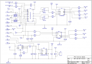
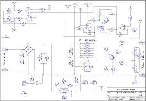
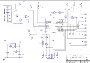
First of all, here is the latest schematic which represents the power supply design as described in this blog and videos with what I believe are the modifications required from the latest round of prototyping and testing.
Here is a video overview of the prototype hardware and test setup as well as some basic tests including load regulation and programmable voltage accuracy benchmarked against a calibrated HP 34401A bench meter.
Here is a video using the software to demonstrate basic set volts, output read-back tests and a benchmark against HP 34401A
I still have the following outstanding issues I want to address before committing effort to laying out a final PCB.
- The “Output Off” circuit needs to be verified to resolve the glitch shown in the video when turning the PSU output on
- Verify remote sense circuit and approach
- Create and test a charge pump to generate a negative supply with a simple regulator, and specifically making sure the diode switching noise does not affect the ADC’s accuracy or stability
- Create a minimum load constant current source for the regulator, and deal with measuring output current and compensating for the current source
- There is currently no output protection of any kind, I need to deal with reverse polarity input (connect a battery the wrong way around to the input terminals), power feedback (connect a battery the right way around and power down the PSU), connect mains AC voltage into the output terminals. Apart from passing thoughts I have not looked at circuit protection at all.
- Verify the accuracy of the current limiting and ADC read-back
In Part 11 I will make further refinements to the design addressing the outstanding items and get a board designed and ordered ready for Part 12 (the final part I hope).
Please do comment and like the videos if you find them interesting. Thank you for watching.


