I said last time I would look at the software and firmware for this post but I decided I needed to spend more time on the regulator to address the DC response issues I had observed, I felt this was more important to get right so this article focuses on that. The good news is, I have achieved good results and I believe the regulator design is complete – at least for the high current version of the module (0-8V 0-8A).
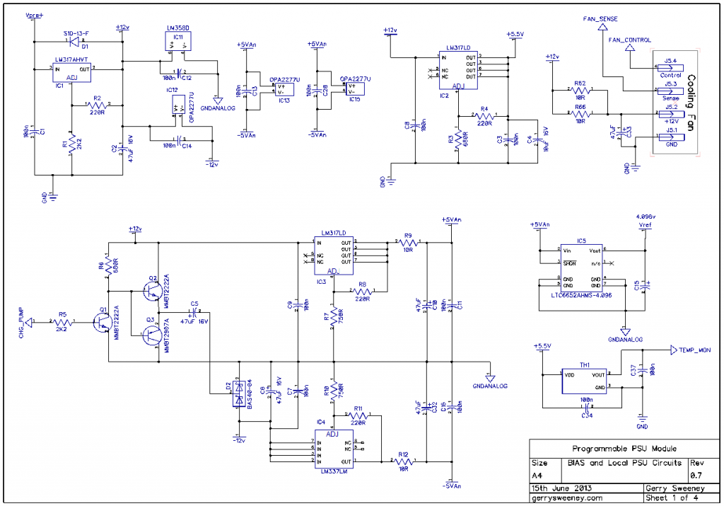
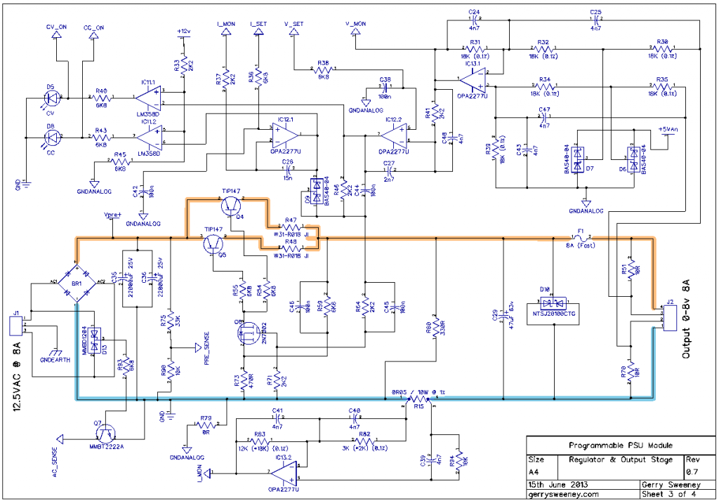
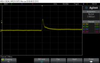
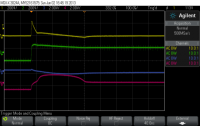
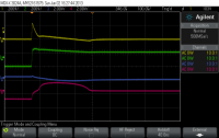
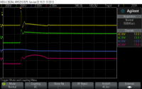
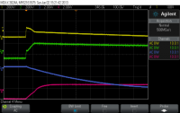
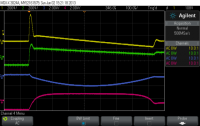
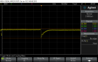
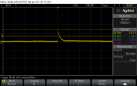
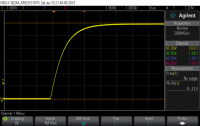
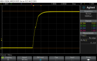
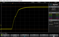
I had problems with the regulator over shooting by about 500mV when transitioning from a high power load to a low power load. There were two main problems, the first was down to the inductance of the wiring on the output, that creates a problem which in turn was amplified by the relatively slow response of the various amplifier stages. I have achieved significant improvement on my previous measurements by tuning response times through the various stages, this simply required lowing the impedance through the various stages to ensure the servo was able to respond more quickly to changes on the output. This was achieved by adding C24, C25, C39, C40, C41, C43, C45, C46, C47 and C48 to the input and driver stages. I also needed to throttle back the fast rise time of the control drive from the DAC to follow behind the response curve of the regulator circuit. These changes mean the regulator now delivers a clean and very acceptable dynamic response to fast-switching load conditions.
The Schematic
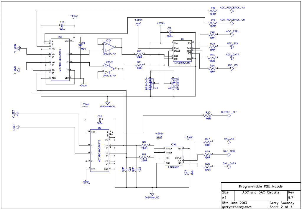
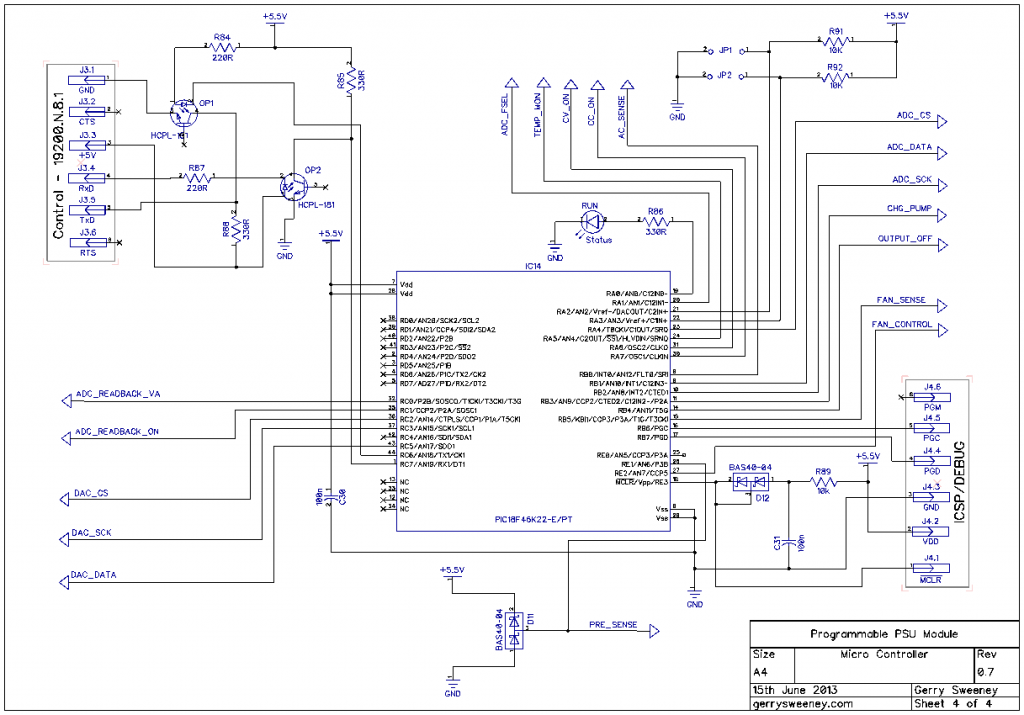
Here is the latest schematic which is at version 0.7 including all of the latest changes. The most significant changes are on sheet 3.
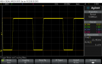
Various Scope Traces from Testing
I now need to lay out the new PCB and get some ordered, I will do this over the next couple of weeks. I will definitely cover the development environment and the firmware in the next post as well as the serial protocol used to control and monitor the module.
Thanks for watching.
This content is published under the Attribution-Noncommercial-Share Alike 3.0 Unported license.

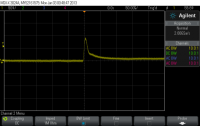
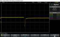
Will boards be made available and possibly parts or just a BOM ?
Hi David, I will certainly get some boards made once I have confirmed they are good. I need to verify the high voltage version also works well so I would wait until then. In terms of parts, I am not sure I am geared up to stock and sell parts, I have not given it too much thought, I guess it depends on the level of interest. Thanks for watching. Gerry
Eager to get one of those boards ;o) Fantastic stuff.
Perhaps it’s easier to read here than on Youtube…
Proportional control itself won’t control to 0 error, so you’ll need to use PI at least. To tune a PI you generally start with the P then do the I. The proportional gain is Rfb/R41, and the integral time constant is 1/(R41*C27), I think. So they should be decoupled.
I’d be surprised if you can’t get a better response. Some suggestions for first attempts at tuning (without Laplace domain theory):
For a PI
1. Tune the P first (put a very large C27 to remove the effect of the integrator). Then find the value of Rfb at which the response becomes unstable (you will probably need a few POTs ranging from 1k to 100k), you’ll want to try about a thrid to half this resistance for the next step.
2. Decrease C27 untill the response is acceptable.
3. Play around a bit more, i.e. start with slightly different Rfb.
For a PID
1. Tune the P for more overshoot (again using very large C27 and no derivative cap)
2. Use the derivative cap to reduce the overshoot.
3. Reduce C27 to reduce error.
Hi Stewart, thanks for the suggestions, I will have another go at tuning base on your suggestions, it should be simple for me to verify but I am not sure exactly what topology you are suggesting. I think you are saying, remove the bypass on R41, put in a large value into C27, lets say 100n, then vary the value of R41 to tune for best response? Where I am confused by this is, its the RC of R41/C27 that define the frequency response no? Gerry
http://mackys.livejournal.com/663317.html This is the topology I suggest… there are more complex ways, that involve more opamps too. If you remove C1 you will have a PI controller, if you include C1 you have a PID controller.
Another way to look at your current integrator circuit is from a purely high frequency perspective (as it’s the high frequency component of the fast transients that we want to control). For this theoretical exercise we assume all the capacitors are short circuits. An opamp with 0 feedback impedance (at high frequency) will be unable to pass through any high frequency error; it will hold everything at 0V. Putting in the bypass capacitor is increasing the available magnitude of the high frequency signal in the vain hope that the opamp can amplify it. Once you put resistor in series with the feedback capacitor and repeat the theoretical exercise at high frequencies, there is now still impedance in the feedback path and the opamp can amplify the incoming signal.
The basic theory of a PI controller is the proportional gain provides the fast response while the integrator removes the steady state error. Proportional gain is just the non-frequency dependent gain. i.e. the proportional gain acts accross the full frequency spectrum (up to the opamps GBP) just like a normal opamp. The integrator only provides substantial gain to lower frequencies, however its phase shift will limit how fast you can set it.
Kp = R2/R1 defines the proportional gain.
tau_r = R1*C2 defines the integrator time constant, or Ki = 1/(R1*C2) defines the integrator gain. If C2 is large Ki is very small, the effect of the integrator is small.
Kd = R2*C1 defines the derivative gain. If C1 is removed Kd = 0, there is no derivative gain.
The frequency response is determined by all of these parameters (as well as the rest of the circuit).
If you want to try a PI to start with:
1. Setting the proportional gain:
Start with a nominal R1 and very big C2 (100n should do, bigger the better) and vary R2 for instability then take a fraction of the unstable R2 (1/3rd, 1/2 around there). I’m not sure what range value it will take, it could be similar magnitude to R1, or an order of magnitude either side (or more). You can also vary R1 at this stage too. You won’t have 0 error, but you should have a fairly fast response with no overshoot or oscillation.
2. Setting the integrator gain:
Reduce the size of C2 until no error.
3. Trial and error:
Try starting with different values of R2. Remember to record what works well…
If you want to try a PID:
1. With no C1 (and a nominal R1), put in a very big C2 again and vary R2 until you get a fast response with some overshoot.
2. Add a small C1 and increase its size to eliminate the overshoot.
3. Decrease the size of C2 to remove steady state error.
4. Trail and error again 😀
Hi Stewart, thanks for the clarification. I had a play around with putting a resistor in series with C27 which seemed to slow down the response time. The response time currently though the entire regulator is about 60uS at the moment which is quite fast when you consider the output has 470uF strapped across it. Adding a series resistance has an impact on the trailing slope (raises it) but does not change the overshoot peak. However the absolute value of C27 does directly impact the overshoot so I will have a play around with this some more and see what I can see. I would appear to have an instinctive understanding of the way this works even though I am not familiar with the terminology or the math. Thanks very much for the info, I will see what I can do with this, I am keen to try because the values I used currently were purely guess work with some trial and error. Gerry
I’m a little surprised it slowed down the response. There may be other more complex interactions occuring (with other plant time constants).
I suggest starting the error amp from scratch if you want to play around in detail. You’re intuitive understand is good! But I find it very hard to just randomly change gains and get a better response. Too much of one gain will mean you won’t be able to put in any other gain.
Hi Stewart. From my early prototyping efforts I found its the rest of the circuitry that has a big impact on the overall response. I would appear to be in a reasonable good place with the current implementation around the error amp, the response time is at the very least comparable with that of a HP/Agilent supply so I am not that far off the mark, it probably does not justify spending too much time on trying to squeeze out better performance at this point. Thanks for the suggestions though, using your approach I have been able to confirm that the values I have selected are quite nicely in the mid point of good response and instability – which is actually nice to know. Gerry
I also forgot to mention that you may need to also consider the effects of C44 and C45. I would remove them for the PI tuning process, then asses again after. Resistors don’t really decrease the frequency response of the circuit, unless you know they are feeding capacitive loads large enough to cause long time constants (whats the input capacitance of your FET?). However they will impact the phase margin of the circuit.
Hi Stewart, the input capacitance of the FET is about 50pF so not that high but I have definitely seen a difference (for the better) with the bypass on C44/C45. Gerry
I also, also forgot to mentionk, these tuning techniques are generally for a step change in command/reference. Since I think you were doing a step in load it will be more difficult!
Hi Stewart, yes I was thinking along the same lines, where I have minor changes the overshoot/undershoot is negligible, I am forcing the issue by spanning about 70% of the range as a square wave drive. The overshoot happens on the rising/falling edge. If I ramp up say over 100uS then I see a little more ringing. With no ramp, the rise time is about 50nS so thats a very fast response, the more current I put through the system the larger the overshoot becomes, and this appears to be because of the inductance of the output leads, I can influence this with a snap-on ferrite which increases the overshoot considerably and into oscillation. This makes me wonder just how much better I can get it by tuning the PID of the error amp. Any, as a I said, the values were guess work so it will be interesting to have another play. Gerry
Correction, the rise time is about 2uS so not the 50nS I stated, I must have been looking at something else!
There may be other interactions going on too to look out for – opamp saturation, current limiter coming in and out.
Also, where does the system measure the feedback voltage, Edge of the PCB or at the load? If it measures at the PCB then you may get an exceptional response at the PCB, but oscillatory at the load. If you measure at the load the inductance of the cables will impact the controller response and you may not be able to get as much controller gain.
The voltage feedback is coming from the load end of the output wires which is probably why the cables inductance has an effect. I have just tried the suggestion, I am using 100n as C27 with a programmable resistor on R41 and I can definitely tune to a response time that is as good as the current value 3.9nF by varying R41 but I cannot really see much improvement on what I already have though. My conclusion then is there are other factors. 🙁
There was definatly the chance of other interactions and other parts of the circuit having more of an impact. Unfortunatly my experience is more focused on using accurate plant models such that you can a tune controller analytically… so it’s always awkward for me seeing heuristically setup controllers.
It sounds like a good response anyway… if it’s on par with the Aglient that’s pretty good.
Hi Stewart, I have played around and got very minor response improvements, specifically recovery time is down to about 30uS which is better than the 50uS I had before, it has not resolved the overshoot which is still about the same magnitude. The new values are R41 is now 680R and C27 is now 4n7 and there is also slightly less ringing than before. Thanks for the feedback. Gerry
I’m glad to have some input (I see what you did there… :P)
Hi Gerry,
For the high voltage version, what method do you want to use for the preregulator? I’m working on something involving multiple taps on the transformer and some triacs to switch those taps… Another way could be whith a variable output SMPS, but that’s more tricky… Or maybe you’re not going to use any preregulator… Although I don’t think that…
Cheers,
Nicu.
PS Sorry for my english it’s not my native language.
Hi Nicu,
I have decided to exclude the pre-regulator for this version. The high voltage version is only going to be rated at 40v/2A so a maximum dissipation of 80 watts in the regulator. I decided not to do anything with the pre-regulator for simplicity. Perhaps a future version, I would like to design a variable Buck SM pre-regulator, but thats for another time 🙂 thanks for your comment and interest in the project.
Gerry
Hi Gerry,
I’ve done some simulations to test your logic for higher voltages, and I came to conclusion that you can’t get higher voltages on the output if you don’t increase the supply voltage for the opamp driving 2N7002 FET. Even more, you can’t get 40V on the output without supplying that opamp with a voltage that excced it’s maximum ratings. Maybe I did something wrong, that’s why I can’t get the expected results. Or maybe you have some tricks in your sleeve, so that you can obtain the expected results. And final, maybe I can’t use LTSpice properly wich is possible cause I’m newbie with it…
Cheers,
Nicu.
Hi Nicu, I am not sure that is the case, I have already tested this I thought but, if that is, all I need to do is increase the value of R59 to reduce the level of negative feedback. Gerry
Gerry,
A thought ( god forbid ) i have just been given a large carrier bag full of lap-top psu from the local
pc-repair shop , whilst a few may be faulty most of them will be fine apart from the DC output lead,
where the cable has failed either at the laptop plug or the psu exit grommit IE where the cable is all ways being bent and twisted. There is 1 X 15Volt 8amp which i put aside for a spare for a vintage Toshiba, but most of the rest are almost all 19V 4.75Amps a further check on a couple showed that they don’t pass the earth line through to the output. My thought is that if i break open the cases i can series these for 38v @ 4.75a or parallel 19V @ 9.5a but clearly wont get the ‘ac’ present signal. I am clearly thinking of using these as the pre-regulator supply…
Hi Span, they would make a good pre-supply I recon. The linear regulator should have enough speed to take out the majority of the residual switcher noise and you can always beef up the low pass filter on the SMP output if noise was an issue, you might also need to deal with shielding too. You don’t really need the AC present signal, what I do with this is measure the frequency in the micro and configure the ADC for 50Hz or 60Hz rejection in its switching filter – in practice though I have not really seen a difference, you can always hard-set this in the firmware. Gerry
Hi Gerry,
now you say that you haven’t noticed any real difference when changing between 50Hz and 60Hz, have you considered using an external clock on the F0 pin to increase the samplerate of the ADC?
Are you using the ADC in continous conversion mode or do you read from it at certain times? In an earlier schematic i can see that you were using it in continous mode by connecting CS to ground.
BR Jonas
Hi Jonas,
The ADC is in continuous conversion mode. I did not consider an external clock because as I understand it, increasing the sample rate effectively reduces the effective resolution. The design needs 21 effective bits at least to cope with the noise floor so increasing the sample rate would probably take me below that. The other thing of course is simplicity, one of the nice things about this ADC is its really easy to use.
Gerry
Hi Gerry,
‘Just a comment for anyone trying to get both the ADC and the DAC updated in one timer ISR in SPI master mode and ADC single cycle operation.
– The ADC needs (CKP=0). That satisfies the ADC requirement for the clock line to be low while CS is pulled down. So:
CS=0
if EOC ==0, CS=1
CS=0
dummy write to SPI2BUF
read the buffer
CS=1.
– The DAC needs CKE = 1.
I used two separate CS lines, no SS, P32MX
Mike
Hi Mike, thanks for the comment. I tried very early on but it was apparent it would not work for my application, I am writing the DAC about 1000 per second, the ADC is only ready to read about 3.5 times per second. I found it easier to bit bang the ADC. Gerry
Hi Gerry, my (selfish) motivation for doing the the ADC/DMA in one ISR was to give my NEW(!!) Fluke 8846A a workout. So I wanted tight timing on the read of the ADC and the write of the SPI. I’m still in the perfboard stage of the project and trying to sort out the accuracy issues vs the DAC, ADC, Vref, board influence etc.
Mike
Hi Mike,
I like that Fluke meter, must try to get hold of one at some point, I like the DM display – very nice…
Gerry
Hi Gerry,
Isn’t the maximum intput voltage on the ADC below 5Vdc? The datasheet says FSet + 0.12Vref ~ 4.7V. Am I missing something? The voltage drop on the diode?
Can you give a little detail on your communication between the psu and the controller/computer?
BR Jonas
Hi Jonas,
Yes thats correct, the max input voltage is rev + a bit. Did I indicate something different?
The communication between the controller and the computer is 8-bit serial ASCII at 19,200 baud. Really simple text based interface, I think I described it at a high level in one of the previous vids. The protocol is of my own invention so is probably not very well thought out – I am planning to cover the firmware and info on the serial protocol. I have not done this so far because the software aspect of this project is in many ways comparible to the early hardware prototypes, very loose and variable, once I have the hardware knocked into shape I will put a bit of effort into the software and make it more industry strength.
Gerry
No, it is just that the protection diodes is connected to 5v and ground. Doesn’t that mean the input to the dac could be higher than 4.7V?
Ok, I’m looking forward to the video then 😉 I’m doing a little prototyping myself – experimenting with your design.
BR Jonas
Hi Jonas,
I see what you are saying. As far as I can tell from the data sheet the max input voltage is Vcc + 0.3v so it should be fine. What happens if you put an input voltage over the reference voltage is it wraps around/overflows the reading, but I believe that electrically this is OK to go to Vcc.
Gerry
Yeah, sorry for my lack of expressing myself in the right way – that was what I meant 🙂
I just misread the datasheet. Thanks.
BR Jonas
Dear
I found your project very interesting i enjoyed reading your almost all post although i rarely read projects post . the way you described about your work is very seek full .today i was thinking to build such kind of project as you did and searching for some base line work already done then i came across your web site during google search but my choice was to use Atxmega32a4u because it have built in 12-bit adc @2 mega sample/sec to reduced bill of martial and cost with compare to complexity i checked the price of main components used in your project and founded these prices on digikey
LTC2402CMS#PBF-ND price is 10.93$
LTC2602CMS8#PBF-ND price is 9.55$
OPA2277UA/2K5 price is 4.28$
PIC18F46K22-I/PT-ND price is 3.59$
where my interst is that why you did not chose a more ecnomical components
for op amp i will chose
NE5532DR price is 0.91$
this op amp have 2 good performance factor which you may had missed in your desgine one is high slew rate 9V/uSEc with compare to 1V/uSec(OPA2277) and second is
Unity-Gain Bandwidth: 10 MHz Typ with compared to 1MHz(OPA2277)
one draw back is the offset voltage is higher then OPA2277 but that’s not the issue when you are using complementary power supply for op amp here i gonna mention that the thing about your over shoot and under shoot may relies to op amp slew rate and Unity-Gain Bandwidth so plz try NE5532 op amp and see what is the real time result hopefully result would be better i saw waveform slide show and it looks like that rising time is very fast so Unity-Gain Bandwidth of OPA2277 is 1MHz and even slew rate is low and you are getting its finel performance its better to chose some better opamp for this purpose opa2211 is another better choice for this purpose
For adc and mcu better choice is analoge devices mcu’s with built in 24-bit adc and even sampling speed is better here is a part # with price
ADUC847BSZ8-5 11.72$ 24-bit adc dual 16-bit dac built in analog buffer and pga for adc so no buffer ic is requiered and no mux even sample rate is better with compare to ltc adc i hope you gonna give a test for this one i just remembered that i have also in my stock so i gonna start working with this one latter i will go for atxmega version for hobby purpose to see what can i get from atxmega
And here about the Atxmega i knew that its adc is not like as they mentioned in data sheet but its possible to get higher resolution using oversampling since it have 2 mega sampling adc built in and i belive that for such that low sampling speed it is also possible to get 20 bit affective result same as with dac also wich have 1 mega sampling speed
In my opinion you wont be agreed for Atxmega for application like this you can chose Kinetis ARM® MCUs with built in 16 bit adc have built in digital filter for adc resolution enhancing analog front in opamp biult in external vrefP and vrefN built in dac and oneof them cost around 3.49$ i dont remember exact part no again if you chose psoc4 series thats is also very cheep 1.45$ and 2.58$ same as Kinetis but low resolution adc 12-bit
any how i will wait for your final project result with firmware detail and pcb . i will be interested if you share your work with me specially one working prototype so i can also compare mine with you for price vs performance vs complexity
Hi,
I could not use the NE5532 op amp because of the offset voltage, I am working down to a precision of 500uV and a 5mV offset is just too much, the NE5532 is more commonly used in audio applications or DC circuits that do not need high precision – I actually started the project using LM358’s which are comparable in many ways to the NE5532. Now if I had designed the PSU so that the regulator was not trying to precisely track the voltage reference then a high input offset might be workable, however, offset voltage in these devices often drifts with temperature so would be less stable over temperature.
I like the look of the AD micro controller you pointed out – it looks interesting, I have not looked at that one before, will probably consider it in a future project, thanks for pointing it out.
Thanks for the comments.
Gerry
dear i found some thing more intersting today that is this ic
http://www.digikey.com/product-detail/en/NAU7802KGI/NAU7802KGI-ND/2769783
and datasheet link
http://media.digikey.com/pdf/Data%20Sheets/Nuvoton%20PDFs/NAU7802_Preliminary.pdf
part no nau7802
some specs
• RMS Noise:
50nV in 10 SPS data output rate and PGA gain = 128
150nV in 80 SPS data output rate and PGA gain = 128
•Differential input impedance 5 GΩ PGA bypass=off, DC
and price is very awesome you will definitely use this ic when you check link of digikey and data sheet
some other candidates are mcp3903 and ads1246.1247.1248 for better noise and more channels input ads124x series can be used +/-2.5 volt for true bipolar operation
no need to worry about current and volt measurement no buffer / multiplexer is required
for dac only economical way is to use dac+pwm at 20-bit resolution and using adc track the dac output for minor INL & DNL error to correct output volt in millivolt range
for op amp offset use it in differential scheme with bipolar supply or use ca3130 whith single supply for over shoot in microsecond time use higher gbw and slew rate based op-amp opa2277 have low slew rate and gbw (gain band width) slew rate is defined in volt/uSec which means that if your opamp have to change its output from 0 to 5 volt so it will took 5uSec to reach 5 volts output level where it need settle time too for verification purpose check if you have one spare opa2277 ic use it on proto board and apply signal generator on input measure input of op-amp and output (with same loading resistor as you are using in output stage to control volt and current) to see the overshoot problem and settling time this parameter is also important when you are using to provide buffering for adc input stage to reduce over all error i hope this will little help you out to make sure that opamp is capable for required performance
Hello Gerry.
When can we expect the release of new parts?
Does anyone have schematic of the pre-regulator such as that Gerry described?
Hi, I am working on the PCB layout and need to build another prototype for the high voltage variant, I don’t want to modify the existing one so I need to build up a second one. The next video for the PSU will cover the firmware and software I am using, that should be in about two weeks from now – I will be away for a week and have some other commitments on my immediate return.
Gerry
Please forgive me for impolite reminder, but someone has to do it 😉
How long are you going to keep us waiting? Put your frequency toys aside for a while and show your other great project as promised.
I love your videos, but I can’t live long on videos about 10 MHz 😉
Hi Johnny, thank you for the reminder, I am aware that I am behind on the project but I have some issues with it that I must overcome before I take it forward. Sometimes its hard to find inspiration to solve the project issues, it has to rattle around in there for a while – rest assured I will finish the project. I will however take this opportunity to add some balance and an equally impolite response here – I produce this blog in the little spare time that I have in my life, I am doing this for free because I enjoy it – the day I become a slave to it though I will stop – period. So while I appreciate many people are following the project with interest – for which I am very flattered and very grateful, I am not working to a specific schedule or deadline – although I would actually very much like to get it finished myself too, so we are aligned there. I think I am pretty much done with the 10Mhz vids now – perhaps just one more! Gerry
The project is excellent, the posts are informative, and I for one am perfectly willing to wait. It’s not like one can have too many bench power supplies. If I need to get another PSU before this is done and I can build one, well, I just end up with an extra PSU.
I love that you decided to use a PC CPU cooler for the heatsink. Too many people ignore them, and end up using overly expensive electronics heatsinks. I’ve found it’s pretty easy to drill and tap holes to allow screw mounting, the base of many heatsinks is certainly big enough to have the room. This can be easier than trying to make mounting posts. Also, for applications where one doesn’t need the fan they can be removed, and there are large heatsinks available for rather low prices.
Hi Carl, thank you for the feedback, I am glad you like the project. Yeah the CPU fan was an inspired choice, I see other projects doing the same now – its nice to be an inspiration. Gerry
Hi Gerry,
thanks a lot for sharing your design,haven’t seen anything like this before,
I’ve learned a lot.
i have some questions:
1.why did you switch from mosfets to darlington transistors? i recall somewhere you said that mosfets are too fast but i dont understand why that would be bad.
2.why did you placed R46 in the voltage loop but we dont have the same resistor on the output of the IC12.1 opamp? is it because you want the current loop to be faster than the voltage loop?
3. what does R59 and R73 do? do they implement some kind of feedforward mechanism?
hope you get the time and do the video on software and firmware soon.
thanks
Ali
Hi Ali,
In answer to your questions.
1. Basically I needed a voltage drive so using a FET driver and a PNP darlington was the “least” component way of doing this using a FET as a driver. Also the PNP transistor is cheaper than the MOSFET I was using. But mostly though, its because the MOSFET needs a higher drive voltage to drive them hard on, you will see in earlier designs I was generating this higher gate bias voltage, but I dropped that to reduce components and complexity. The PNP solution works really well, you can see in the performance tests for current and response.
2. R46 provides DC current relief for IC12.1. Basically, when current limiting kicks in, IC12.2 will try to compensate but R46 limits the current which is being shunted away by IC12.1 via D9.
3. R59/R73 provide the driver with local negative feedback, in essence turning Q8 +Q4/5 into something like a linear-ish voltage amplifier.
Gerry
thanks for your answer
I think the complexity was because you had used an n-channel mosfet. it could have been much simpler with a p-channel mosfet or wouldn’t it?
On the other hand Power dissipation capabilities of mosfets are much better, 50W for tip127 in comparison with 130-150W for irf540.
i dont get your point about the higher drive voltage. first we dont want them hard on since it is a linear regulator and second of course they have a threshold voltage higher than the bjts but once you get past that voltage the current rise very rapidly and we dont need that much voltage.i think i miss understood you here.
thanks again
Ali
Possibly a P-channel MOSFET would have been simpler but I am not sure they are as easily available (cost wise) or as reliable because of their construction (although I am no expert). You generally do not see P-channel MOSFET’s in linear designs for this reason. I think the TIP36C is good for 125W from memory which relates as much to the physical packaging as anything else. I have a low voltage, high current PSU design goal, and for a MOSFET I would need drive capability to get a low RdsOn, which generally means a gate voltage of about 10V above the source voltage. In the low voltage PSU mode, (12V drain, 8V source under full 8A load) I simply did not have that headroom to get a low enough RdsOn so the BJT in this case works much better.
Gerry
I couldn’t find anything that proves your point about reliability in p-channel mosfets.i think the defect was in earlier versions. but yeah, they are more expensive
thanks for your answer.
Ali
Yeah, perhaps my knowledge is out of date or I imagined it, its just I have not ever seen a P-channel FET used in a linear regulator before…the N-channel and BJT’s are proven solutions I suppose. Gerry
Why not use one of these current sensors instead of that expensive resistor.
http://www.allegromicro.com/en/Products/Current-Sensor-ICs/Zero-To-Fifty-Amp-Integrated-Conductor-Sensor-ICs.aspx
They are about half price or less, no power loss and about 1% accurate and isolated from power path.
Then about the choice for a different micro. Also ti produces a couple of msp430 with up to 7 24 bit adc’s builtin.
Those current sense IC’s look really interesting, I think I am going to grab me a sample and see how they work out. I have some issues with the current sense resistor – apart from cost, mounting them is an issue and one of these IC’s might solve that problem, I will keep you posted, thank you for the the suggestion. As far as the choice of the micro, yes thats a possibility but I know PIC’s and I did not want to learn another architecture for this project – I am aware of the nice on-bard stuff you can get with them – PSoC too, but thats a new platform, new tools and new project for another time 🙂
Ur welcome.
And about another micro, somewhere in the beginning of the psu series, you gave a valid reason for starting with a pic, but because there were some other suggestions of micro’s here, I thought I chime in another that had higher resolution adc’s .
PSoC’ are indeed another game, while the switch between a pic and a msp430 seems more like the same game with some rules changed.
Anyway good luck with the acs series as I am thinking about using some as well.
Hi, yes I really like the look of the PSoC devices, they look really interesting to play with. Not sure I want another learning curve just now though 🙂 Thats FPGA’s and PSoC’s on the shopping list….Gerry
Hello Gerry.
Will something like that (see the picture at link: http://imgur.com/IYUmhw3) work with your device? (yeah, it’s based on n-p-n structure while you using p-n-p transistors and probably somebody can change the schematic for p-n-p). I still can’t find schematic of good pre-regulator.
And.. where is new part of epos? 🙂
Hi, thats more of a switch mode, the kind of pre-regulator I need is a buck-type. I have just gotten hold of a bunch of inductor/transformer cores to play with to see if I can some up with something simple and effective. Still working on the next video for the PSU, I ran into some layout and physical construction issues I need to resolve. Still very much in progress. Gerry
G’Day Gerry,
Hey well done so far on this design. I have been following with a great deal of interest.
Count me in for 4 of these modules if you sell them, even if they are just the PCB. Heck I would get the next revision if I could, just to play along at home.
A few questions for you squire if you don’t mind…
Have you thought of using an resistor array for your digital isolation?
e.g. http://au.element14.com/yageo-phycomp/yc248-jr-07100rl/resistor-array-8×0402-5-100r/dp/1377045
I can’t recall it being discussed in your videos, however it seems that all connectors are inaccessible once the board is mounted in a chassis. If for example these are mounted in a 19inch rack unit, it would be difficult to unscrew the module to gain access to the connections.
Admittedly there are connectors such as http://au.element14.com/fci/20020618-m031a01lf/terminal-block-pluggable-3pos/dp/1788456 which can be utilised easily enough.
However the serial and ICSP header are dead centre, perhaps if they were mounted behind the main filtering caps they would be vastly more accessible, as too the status LEDs.
I apologise, I don’t know your grand intention and really I am inspired by this project and have purchased a great many components and evaluation boards, heck even a pickit 3. Sorry I am Atmel raised, and learning PSoC ATM.
I see this as a fantastic education series, and even if you don’t release a kit, I think I will still endeavour to complete the project in house as many ideas you have presented are very sound.
Even though I realise you are trying to keep board real estate minimal, have you considered the advantage of using board route outs to mount the heat-sink mounted components. I recall seeing it used on old telco equipment, Hameg seem to have used this technique here is a video showing what I mean…
http://www.youtube.com/watch?feature=player_detailpage&v=4xlQ9VPg6Y0#t=327
I have been following along with great interest, as I feel this represents one of the best examples of solid design, and your willingness to modify as you go along demonstrates excellent design flexibility, can’t half tell you have a programming background. A lot of hobbyists and pro’s could learn from this technique.
Anyway, you are doing great work. Count me in for a sale of your product. Remember there are heaps of amateur experts and few field experts. Keep your chin up and I am looking forward to your next episode on this truly awesome project especially the XCode.
On your work with the Rubidium Standard… Look up RDDS or reverse DDS, not my work but an excellent way to create a super clean 10Mhz reference.
G’Day Todd,
Thank you for your comments and kind words. I believe that the next board revision should be the last one (he says), once I have tested and verified I will get some boards made.
I have not considered the resistor arrays while I am prototyping, its very convenient to be able to break into a digital line if you need to. I have optimised the board layout for hand assembly where I can, I might compact it further later on and then the RA’s might be a good option.
The aim is the modules connections will be internal only, they would be brought out to the front/rear panel as required. Most likely I would solder the main power wires directly to the board. The screw terminals are easy in the prototyping stage. Right-angle pluggable connectors would be an option.
I can’t route the ICSP and Serial connectors because the high power tracks are fencing everything in but this should not matter once the modules are installed in the final enclosure.
I have recently considered board route outs, but the thought of two boards, and especially some kind of board interconnect has so far left me avoiding that approach.
Thanks for your comments on the design. I am not a pro, I have never done electronics in any real commercial sense, its always been a side interest for me – but something I enjoy doing. I have been designing and writing software for business applications for 20+ years, mainly in C++, and have tackled everything from kernel drivers to database driven applications so I have learned a thing or two along the way. None the less, embedded is different and PIC’s have always been by go-to micro – sorry about that 🙂
I was thinking about a VCO phase locked to the RBS but as it turns out, the output from the RbFS is actually pretty good for what I need. If I were to try and use it to multiply up to microwave frequencies I understand that would be more of a problem and RDDS might help there. Thanks for the suggestion
Gerry
Hi I would like a board when you have them ready
thanks Chris
Hi chris, will do, thanks.
Are your work in github or any other sourcecontrol site?, easier to download and peruse schematics and firmware.
Hi, not currently, but I will put the source code somewhere accessible once I have published it and done a video walkthrough. Gerry
Hi Jerry,
Do you think you may be getting back to this any time soon? Not that you have any thing else to do but design a PSU for the Internet community. 🙂
Just consider this as friendly encouragement, and put me down for a board when they are available.
Take care and enjoy the holidays!
Steve
Hi Steve,
Yes absolutely, work has been very busy over the last few weeks so finding time has been really difficult, I intend to rectify this in the new year. Thanks for the encouragement and happy holidays.
Gerry
Hi Gerry,
‘Hope you are enjoying the Holidays.
I’m just getting caught up on the changes & improvements in this episode and find I really learn something new and clever each time. One quick question: On the most recent schematics, the PWM V_Trim circuits from previous versions are now gone. Are these not needed anymore? If true, I assume it was because they were simply not not necessary due to the recent improvements. Can you comment? I apologize in advance if I missed it.
Happy New Year,
Mike
Hi Mike,
Yes you are correct. When I introduced the PWM trimming I added this as compensation for input offset “current” on the LT1301. When I switched to the OPA2277U op-amp the input offset current was vastly improved and trimming to compensate was no longer needed so I was able to simplify the circuit. When you are working at these sorts of precision levels choice of op-amps becomes quite critical but there are so many options to choose from you often get led to the right part by tackling specific issues and addressing them. For this design very low input offset voltage and current characteristics are very important to maintain the integrity of the balanced front-end amps. Glad you can learn something from it though, thank you for watching and commenting.
Gerry
Hi Gerry, I’m rolling my own bench PS and went through a very similar path. My design was based on a NPN pass BJT, then a P-FET, and then a paralleled TIP127s. It is still on the protoboard, but the voltage feedback is also very similar to your previous versions so I benefited a lot from your improvements. I will be waiting for your next update on this! If your page view stats go up it’s just me hitting the refresh button on the browser 😉
Regards from Spain!
Ivan
Hi Ivan,
Glad you liked the series, the regulator is sold and fast and reliable from what I can tell, I like the design because the “tube like” local negative voltage feedback which really puts the circuit into a linear region which helps massively with stability – I can tell you I tried lots of configurations and where I ended up works really well on the low-voltage-high-current design. Now I am working on the high-voltage-low-current version based around the exact same design and I hope that will be as stable. Cheers for the extra traffic 🙂
Hasta la próxima vez
Gerry
Hi Gerry,
Really love this project!!! (Count me in to purchase bare boards, kitsets or whatever you choose to sell when you’re ready. FYI, I’m about as far away as humanly possible while still living on the same planet. Go on… GUESS! LOL)
Anyway, something you might want to consider is what will happen when some idiot (take me as an example) goes and connects the output directly to a car battery. And then let’s REALLY make it tough by connecting the battery BACKWARDS .
Obviously, this will cause your friendly fuse to ‘let out some smoke’ (which is just what it SHOULD do). However, the voltage error amp (IC13.1) is still in circuit. Depending on manufacturing tolerances of components around this amplifier it’s remotely possible for it to start driving it’s output (i.e. V_MON) to the -5V rail. I have a sneaking suspicion that IC6 would start complaining in that case? Maybe a current limit resistor and diode clamp to ground between IC13.1 and IC6??? Or maybe another BAS40-04 wired similarly to D6 and D7 to clamp both ends? Another ‘option’ might be to take the IC13.1 input from the opposite side of the fuse? (However, this method might lower the overall accuracy due to contact resistance and fusewire resistance not to mention that it takes a finite time for the fuse to blow)
There IS, of course, a third option… Simply tell idiots like me that we really should AVOID connecting car batteries in reverse to the output in the first place… (But that’s just too easy… LOL)
Anyway, GREAT project!!! I look forward to seeing your next article! (In MY mind, it’s about ready for the official ‘boxing up’ and a nice code description)
Hi Trev,
Thanks for the feedback. Yeah thats a good point and I think you are right. Originally I needed a low impedance drive in the path to reduce noise but since added a buffer (i.c. 15) on the front of the ADC so I should probably put some series resistance and a diode clamp on the I_MON and V_MON lines. Once I have finished the modules I will do some *harsh* testing on them 🙂
Gerry
Hi Gerry,
I’m about to ‘show my ignorance’ once again. I’m the first to admit that my knowledge is a LOT less than ideal…
The two series pass transistors (Q4 / Q5) each have a stated hFE of 1000 @ IC=-5A and 500 @ IC=-10A. (See https://www.fairchildsemi.com/ds/TI/TIP147.pdf)
Let’s assume a value of 1000 since the pair will ‘share’ the output load. (Although it might be a little more than that)
The PSU is stated to have an output of up to 8A which implies each series pass transistor is supplying half that value (ie 4A or 4000mA)
In order to provide that output they each require 4mA of base current.
Given an AC supply of 12.5V and taking into consideration the 6k8 resistors on the base of each transistor (R54 / R55), I find it difficult to see how enough ‘oomph’ (base current) is available? Even if I was to directly short the drain & source of the FET I’d have difficulty seeing more than 2mA base current in each transistor which would imply a 4A maximum output.
Assuming I’ve not made some ‘fundamental mistake’ (huge sigh!! I wish I knew more ‘stuff’), then I’d expect R54 / R55 to be HALF their current value and perhaps even halve that again to give a decent margin. (eg: 6k8 -> 1k8). Whether this would mandate any changes in other areas is FAR beyond my skillset.
Hi Trev,
According to the on-semi data sheet which is more specific, the hFE of the device is 1000 absolute minimum, in practice though it can be (and obviously is) much higher than that and I believe in this configuration it is, although I have not checked the upper bounds of what that might be. In testing I was easy getting to 8A without saturating any part of the drive circuit based on the current values. However, a crappy TIP147 might challenge that, I see no reason not to increase the base current in the circuit to assume that the gain of the output device is only 1000, but the values of R59, R64, R71 and R73 would need to be re-worked. My original prototype and testing was based on the high voltage version (0-40v 0-2A) which is where the original values came from, I then worked on the low current configuration and found I did not need to change anything which is good for the BOM. When I do the next part I am looking at the high-voltage configuration again so I will be playing around in this area, I will make a point of demonstrating the measurements of this part of the circuit. Thanks for the feedback.
Gerry
Gerry,
Here’s another silly question from me…
Pretty much every Lab PSU schematic I’ve seen is inherently ‘single ended’ in nature. They can active drive the output to INCREASE the voltage, but they’re unable to actively DECREASE it.
The simple fact that there must be some inherent finite delays in the feedback / control circuit ensures that there will be some finite degree of overshoot if the load steps up. Furthermore, if the load suddenly drops (to near zero?) for whatever reason, another overshoot ensues and it takes a finite time for this to passively decay.
I’m seriously beginning to wonder if it’d be practical to use something like a Class-AB amplifier output stage instead of the single-ended series pass transistor?
My ‘gut instinct” is that such a design could be made far more ‘tolerant’ of the (sometimes ridiculous) levels of capacitance and inductance that we place on the PSU output terminals.
Just for fun, I might do some ‘experimenting’ (LTSpice first and then with some silicon).
Hi Trev,
For the most part this is simply down to cost I think. What you describe is a perfectly valid PSU design, in fact if you do it right, what you end up with is a constant current source/sink device which would work equally well as a DC load….would be interesting to play around and see how useful that would be in practice. Of course you could not get all the way to zero although you could get pretty close if you use MOSFET on the sink side. Never really thought about the capitative load although my initial instinct would be you could still have problems, just like in an audio power amp if you try to drive capacitive loads.
Gerry
Gerry
Obviously, such a device would cost more in parts, but I doubt it’d be a HUGE difference.
I already have the zero volts output issue sorted… Just like your typical audio amplifier, I’m using a split supply. An interesting side effect is that the whole PSU becomes ‘bisexual’ since ‘it can swing both ways’.
Another interesting ‘side effect’ is that it can become a crude form of AWG by modulating the V-Set input accordingly. (Obviously, any bandwidth limits of the Class-AB would limit output frequency capabilities).
I’d guess that the fixed load (R60 in your design) would be implicitly provided by the quiescent current in the output stage.
Any output filter caps (eg C29) become less important. (They’re mandatory on a PNP LDO, but you don’t often see them on a split supply Class-AB amp… LOL)
I’d envisage something like an Allegro ACS712 hall-effect current sensor. (1.2milliohm and bidirectional!) instead of a resistive shunt sensor.
The firmware by itself would be intriguing to say the least. Especially if it included the ability to function as:
– Lab PSU
– Programmable load (that can source or sink)
– AWG
– Other???
Anyway, enough of my ‘mindless chatter’, I need to get designing!
(Aaaaargh, NOW look what you’ve made me start!!!)
Quick question. Did you have a chance to test your design for spikes during startup?
Hi, yes there is a small spike at power-up but once you use the firmware controlled output on/off its smooth with no spikes at all..Gerry
Gi Guys
Great project i enjoye the comments.
It is a year or so since the project finished and i would like to know
if the pcp ths still available and where can i get a set.
Thanks for your coorporation .
Herrold
Hi Herrold, the project is not quite finished yet, I know its been a long time but there is still more work to do. I will finish it one day…Gerry
Hi (again) Gerry.
Have you considered extending your DAC->ADC feedback system to include the entire loop?
This would form the basis of a VERY good ‘calibration’ routine in the firmware!
(It might even allow you to use lower spec opamps / lower tolerance resistors in some places)
I’d also suggest inclusion of a firmware routine to allow calibration against an EXTERNAL device eg: Some users might have access to a calibrated 8.5 digit DMM! (I’m envious!)
I’m NOT saying you should eliminate the existing DAC->ADC feedback at all. I’m suggesting an ADDITIONAL option.
Hi (again) Trev,
Its already in the entire loop, it has remote sense capability in the design. When the voltage is being set the ADC ensures that the reference voltage is as close to the required value as possible. Once in read-back, its reading what the front-end sense amp is seeing which is the remote sense value. Maybe I am not understanding what you are suggesting?
Gerry
Sorry that I was ambiguous. I tried to ‘shave down’ my atypical ‘novel length’ posts…
Let’s assume that we have the PSU set for 4V of output (thus implying that we’re setting a VRef of exactly 2V).
In a perfect world, with perfect components, the feedback loop will do whatever it needs to in order to make the output exactly 4 Volts, but we live in an imperfect world with imperfect components. It might help my illustration by intentionally exaggerating these imperfections.
Let’s assume that IC12.2 has a (ridiculously large) input offset voltage of 500mV! With our hyper accurate 2V of VRef being pumped into pin 5 of IC12.2 our device will do whatever it takes to attain an equilibrium. However, with 500mV of offset, this equilibrium will occur when pin-6 of IC12.2 has 1.5V (or perhaps 2.5V depending on the sign of the opamps offset voltage). Thus, when we set VRef to 2V, our actual output is 3V (or perhaps 5V) instead of the expected 4V.
There are also errors produced if the gain setting resistors around IC13.1 (R30,31,32,34,35,39) are not perfectly matched…
What I am suggesting is to include a calibration routine into the firmware that can characterise and save these inaccuracies (in the microcontroller flash) and then utilise these ‘cal points’ (with interpolation as required) to ‘trim out’ the introduced errors.
Going back to the (hypothetical and ridiculously large) 500mV offset error in IC12.2, our ‘readback’ voltage of the V_Mon output would be 1.5V (2.5V) thus indicating an output of 3V (5V) at the output. However, our saved ‘cal’ data would apply a corresponding 500mV offset to the V_Ref generated by the DAC in order to eliminate the error in the feedback loop.
For those lucky few with access to a calibrated, high resolution DMM, the calibration routine could also prompt the operator to ‘trim’ the DAC output at a few selected values (eg: 0V, 125mV, 250mV, 500mV, 1V, 2V, 4V and 8V).
A similar routine would allow calibration of the current control loop. (The operator could possibly be instructed to short out the output in order to ‘calibrate’ the current feedback loop)
Your existing ‘DAC-trim’ subroutine would still be used at run time to accurately set the V-Ref and I-Ref points, but these values would be subsequently ‘biased’ up or down by the cal values stored in the PIC flash!
In theory (ugh… Theory!!!), I would expect the PSU could thus be able to ‘trim out’ a significant proportion of loop errors that were induced by ‘lower spec’ components within the loop. Heck, you could even use 10% resistors to set the geain and calibrate out any ‘static’ discrepancies! The primary requirement then shifts to requiring components with a great TempCo rather than with a great initial accuracy.
I hope that better illustrates my thought process?
Hi Trev,
Yes I see what you are saying now. So yes that would be possible but in my earlier experiments I found that lower spec components in the control loop did not yield linear results in terms of error offsets, especially as the opamps get pushed outside of their linear range close to the rails, so for that scheme to be accurate you would need to store calibration points throughout the range and take into account other factors like ambient temperature all of which have impact the specs. I selected op amps with very good specs for both input offset voltage, input offset currents and tempco and decided in the design I would make the control loop accurate enough to achieve the desired resolution as a linear design, then all I had to do was concentrate on generating a precision reference to feed in.
I also really liked the idea of doing away with any need to calibrate in the first place, so with a reasonably selected voltage reference source and precision low tempco resistors in the front end divider thats the result I got which I was quite pleased with.
I am sure your suggested scheme could be made to yield good results too though..
Gerry
That’s a great aspect of your design Gerry…
It already incorporates the pertinent hardware design aspects that give it a pretty good level of accuracy right from the outset…
For those ‘finicky few’ who elect to take it one step further, it’s simply a matter of a firmware update to take it to ‘the next level’.
You’ve no doubt analysed all those Agilent E36xx supplies that you’ve repaired. As you’d expect from Agilent (or whatever the heck they’ve chosen to call themselves this week), they are a very accurate unit despite the fact that they’re only using TL072 class opamps!
With YOUR design that’s employing a far better class of opamp at the outset, the potential is there to ‘blow away’ those Agilent supplies in terms of raw accuracy. Those who aim to actually construct one of your supplies , has the option of ‘tweaking’ it to suit themselves. In my case, I’ll be wanting to do things like using VERY low tempco resistors. I don’t care what their ‘initial accuracy’ is, providing their long term and temperature related drift is (to use a kiwi phrase) bugger all!
It wouldn’t surprise me if some of our ‘volt nuts’ cousins are intending LTZ1000 style ‘enhancements’. (Sure, the LTC6652 is good, but the LTZ1000 is just… ummm… ‘gooder’ )
Give yourself a ‘pat on the back’ for this one!
Very interesting project, learned a lot watching your videos.
I hope we get part 15 any time soon! Definitely want to build one 🙂
I will do my best as soon as time allows. Thanks for the comments. Gerry
Excellent work on the power supply project! Can’t wait for another episode.
I built a poor mans version of your Rubidium Distribution Amplifier project just using a 8663-XS. Much cheaper solution as I only needed to add a 12v supply, no fan, etc. Box never gets very warm and the signal is very smooth. Just working on a 16 bit DAC adjustment circuit for the 8663-XS. I will post photos once I am done. Not sure how to calibrate it as all my equipment is waiting for a frequency standard to be accurate. (chicken/egg thing)
On the power supply project I was wondering it you looked at other low offset op amps. ie the MAX44248 http://datasheets.maximintegrated.com/en/ds/MAX44248.pdf Only reason I ask it it’s ~$2 for a dual vs ~$5 for the OPA2277. Seems to have similar specs, unless I missed something obvious.. Always looking to save..
Do you think that would be a favorable alternative?
Hope to see Episode 15 soon. Keep up the good work.
Dave Boechler
Hi Dave,
that looks like a pretty good alternative to me, would have to test it but on the face of it not bad. I would say the prices of these things vary enormously, the OPA2277 is $1.7 at qty of 1000 according to the TI web site.
Gerry
Hi Gerry,
As I mentioned a while ago, I am working on a similar project. I am having some annoying problems that I am having a hard time over-coming. I am using an Arduino but just to display voltage and current; VSet and ISet are done just with a voltage reference and then 2 pots to the respective OpAmps. I monitor current on the high-side using a TI INA225. http://www.ti.com/lit/ds/symlink/ina225.pdf Everying works fine without the Arduino connected. With the Arduino, however, the thing oscillates like a song-bird. It’s probably a layout issue – I’m still at the veroboard stage, but I thought I’d ask. Where does GNDANALOG meet up with GNDDIGITAL in your layout?
Thanks,
George
Hi George,
You ideally need to adopt a star-ground topology ensuring that your analog and digital grounds all terminate at one central point, as a general rule in a PSU like you describe I would make this happen right at the point of the GND side of your bulk supply/filter caps which should also have a very low impedance path to your load – that part is especially important. That being said, your circuit may be inherently unstable and the noise from the Arduino is just pushing it over the edge into oscillation. I would look at your feedback/servo circuit and de-sensitise it to the frequencies its oscillating at. Your output load and the way that and your output sensing circuits are wired with respect to the load all matter a lot. By far the most challenging part of my PSU project was stabilising it, took a lot of experimenting until I gained an instinctive feel for where and what to look for. Even badly wired on a breadboard, so long as you have goo low impedance ground paths you should work on stabilisation first. Hope that helps
Gerry
hi Gerry,
your project is very interesting. Compare your schematic, in the former version 0.4a, it seems R4 and R5 set the voltage gain, but i did not see them in your new version schematic. Then how can you extend the output?
Hi,
Yeah its a bit more complicated, basically you set the gain around IC13.1 via R30,R31,R32,R34,R35,R39. Thank you for the feedback.
Gerry
HI Gerry
I am working on a high power test supply to use in my new lab that will give out 0-800V and 0-100A current and having watched all the videos etc for this project i am sure it will be a great way to control my PSU design,
Can you tell me if the PCB’s or a complete PSU are for sale yet and can the source code for the PIC and PC test program be downloaded from the site somewhere ?,
Many thanks
Dave
Hi Dave,
Blimey thats a big PSU – 80Kw, whats it for? I do not have the final PCB’s yet, I have he next small batch which fixed all the last errors but I have not yet built them up, the project went on the back-burner because of other commitments. I have to clean up the source code and replace some proprietary code before I make the source available, I will see if I can get that done and post it somewhere.
Gerry
HI
YES that sounds good, keep me updated,
The power supply is for testing inverter power systems, the power supply will run from a 415V 3 Phase supply with a PWM power stage for the pre regulator feeding 18 of 48V 165F Ultracapacitors to give a massive power backup for high peak loads and then your control system for the output control, it will be a massive unit built into a larger 1.5M high server type case, i have ordered loads of parts already and will start to do some tests with these ultra capacitors as soon as they arrive, i have all sorts of things i can use such a high capacity power bank for like a rail gun etc that can tap into the power via a high power switch, i have ordered a couple of 3000 Amps contactors as part of my kit list, one is for power bank isolation and the other to allow for the power to be fed into loads for these extra experiments i want to try,
Many thanks
dave
Dave,
Sounds great, would love to see some photos of it when you have it built.
Gerry
Hi Gerry,
Happy New Year! ‘Just wanted to let you know I am have almost too much fun working on your PSU design. Prototype #1 is breathing. I just finished writing 18 basic software commands to write and read from the ADCs and DACs. Here’s a quick rundown:
– pic24FV32KA304 …. 5 volt, 16 bits, MPLAB X
– 8 volts, 7.5 A output
– Ohmite series 10, 4 wire, 4.5 watt sense resistor. I picked that one so I could bend the two sense wires back into the analog plane.
– The AC, rectifier circuits and op-amp supplies are still off board.
– Arctic Alpine 11 Plus cpu cooler w tach/pwm
– Indigo Terminal Emulator for I/O at the moment.
Other than that, the design is essentially yours. I used larger case size MUX chips and a DIP OPA2227 in deference to my eyesight. It’s on a 3″ x 5″ PCB not including the power input circuit. Now begins the programming for best resolution and precision .. I’m not a good programmer.
If you’re interested, I’ll be happy to send some photos. ‘Just let me know how to do that. Thanks again .. I’m having a great time working on this project.
Mike
Hi Mike,
Happy new year to you too. Sounds great, would love to see some photo’s, send them over by e-mail if you like. [email protected]
Gerry
Hi Gerry,
A quick update regarding stability:
– MPLAB X in debug mode w/ICD3
– Indigo Terminal Emulator
– 7.0 volts into a 1 ohm resistive load
– Strictly hardware feedback, no digital/software correction yet
– Fluke 8846A in statistic mode
Range: 6.999472 volts to 6.999558 volts, SD 11uV, 8900 counts (~ 30 minutes)
…. I’m very happy with that!
In your blog, you noted that you tested stability into a “capacitive load”. How did you set that up? I’d like to try that as well.
TODOs:
– Fix a significant noise issue from the PIC PWM to the fan.
– Settle on a GUI. Given a thorough look online, you seem uniquely adept at using Qt as an interface with MPLAB X. No one, as far as I can see, has that working but you… well done. I’m looking into a graphical interface vs 2 LCDs with a touch pad and some encoder wheels.
– V2 of the board. Given that this a floating supply, is there a chassis bond anywhere i.e. the front end of the transformer section?
– Box it up.
Thanks,
Mike
Mike,
Thanks for the update, sounds like you have made good progress.
Gerry
Gerry, can I ask that you take a quick look @ sheet 1 of your schematic.
My math seems to state that the resistors (R3/R7/R10) on your ‘317/’337 regulators don’t seem to match up with the +5VAn, -5VAn and +5.5V rail values. Your +5.5V rail looks to be generating +5.11V (which is actually a GOOD thing) and your +/-5V rails look to be generating +5.51V (which is also good in that the opamps have a little more ‘headroom’). Perhaps it’s just the labeling that’s confused me? [+5VAn -> +5.5VAn, -5VAn -> -5.5VAn, +5.5V -> +5.1VDig]
Have you ever taken a look @ the LTC2404/8 ADC?
It would allow you to totally eliminate IC6 and therefore the additional 100ohm resistance it inserts into the path. Also, if you used the ‘2408, (which has the same footprint as the ‘2404), you would have ‘spare’ channels available for monitoring a pre-regulator). The ‘2404/8 SDI pin could be tied directly to the 2603 SDI pin so it wouldn’t require additional MCU pins (even though there’s plenty available). I’d expect the overall BOM cost to remain about the same.
There’s also a ‘2604 DAC available that has additional channels (which could be used for a pre-regulator if desired). However, using this part would simply increase the BOM cost in your current design that doesn’t need any additional DAC channels.
I’ve assumed that TH1 (on sheet 1) is something like a Maxim DS60? Is it intended to measure ambient? Or is it thermally connected to the heatsink?
You might find it useful to add a pullup resistor to the output-off signal.from the MCU. The LTC2602 DOES ‘glitch’ a bit upon power up so it’d be wise to force IC9 to select the grounded outputs as early as possible. On power up, the PIC pins will all be high Z inputs until they are instructed to become active outputs by the firmware. This would allow any glitch from the DAC to pass through to the regulator. Perhaps the output off signal should be ‘active low’ with the 4053 inputs swapped?
(Personally, I think the ideal LAB PSU should have an electromechanical [relay] based output off rather than just instructing the regulator to deliver 0V at 0A. Having D10, C29, R60 etc still connected to any load when the output is theoretically ‘off’ is potentially worrisome to me)
Can I ask why IC15 (OPA2277) is setup as an input buffer to the ADC instead of an output buffer for the DAC?
It appears that the DAC outputs each pass through two integrators. I’ve assumed the first one is to implement your DAC dithering and the second one with a longer time constant (inside the regulator itself) is to control PSU overshoot.
As mentioned above, I’d remove IC9 and use an alternate output off method. I’d then merge the four integrators into two and alter the firmware based dithering to suit.
Footnote: I’ve viewed DOZENS of lab psu schematics on the web and yet I still keep coming back to your design. I guess that’s because yours is the closest I have found to what I consider my ‘ideal’… Good work! I’m patiently looking forward to seeing part 15 in this series.
Hi Trev,
Yes the labelling is wrong, I was using simple preferred resistor values, so the voltages are not critical, and so are a bit higher than the nominal.
I had not looked at the LTC2404/8 ADC before, looks like an interesting part, and as you say, could be made to work and could eliminate IC6, but I would still need to do something with the output off.
The temp sensor is an LM35 and its strapped to the heatsink, specifically there to measure the running temp of the output device
Yeah I could probably tweak the output off circuitry around a bit, a pull-up or as you say invert the logic.
The ADC needs a very low impedance source to maintain accuracy, so its a simple voltage follower to get the drive current needed to allow the cap in the ADC to charge properly. Accuracy goes to pot without it. You will see on the ADC you suggest they bring the output of the mux out on a pin, that would be for the same reason, although you would save on one element of the op amp there.
The outputs of the DAC’s drive the two integrators which are in the feedback loop of the V and I regulators, these integrators are the heart of the regulation, the integrators play no part in the dithering but the simple low-pass filter R38/C38 and R36/C42 smooth out any dithering ripple from the DAC.
Gerry
Using a 2404/8 removes the need for IC6 irrespective of the output-off handling. (That’s IC9 rather than IC6). However, I also alluded to possibly changing the output-off to be a relay (which would thus eliminate IC9 too).
While I completely understand that you need IC15 as a buffer, it’s my suspicion that it’s only needed for the DAC readback os I-Set and I-Set. The remaining two inputs to the ADC (V-Mon and I-Mon) are already the low impedance outputs of existing opamps and therefore should not require buffering. By rearranging IC15 to become a DAC output buffer instead of an ADC input buffer, you’d still be feeding the ADC with the low impedance source, and you’d be able to use the same low impedance source to drive the regulator itself thereby possibly slightly improving the accuracy within the regulator section too.
BTW, the examples in the 2404/8 datasheet in front of me only show ‘gain stages’ between the mux output and the ADC input. In all other examples (where the gain is implicitly unity), it shows a direct link from mux to ADC. It’s noteworthy to mention that the ‘on’ resistance of the 2404/8 mux is in the same ballpark as the 4053 (circa 120 ohms with VCC=5V), so I’d agree it might be useful to include a single voltage follower between mux and ADC. Sounds to me like a good justification to use an quad OPA4277 (or similar) instead of a dual OPA2277?
I’ve (FINALLY) ordered most of the components I’ll be needing for the build. I deviated a little since I’m including a controlled pre-regulator as well as electronic input transformer tap switching (using SCRS + optos similarly to the HP PSUs you’ve repaired)
I’ll be using a low end Atmel as the primary CPU with similar opto-isolation. (No real reason – Just felt like it). The whole PSU ‘module’ can be run as a standalone PSU unit by plugging in a couple of rotary encoders and a simple HD44780 style LCD, but can also be combined with additional ‘clone’ modules along with an ‘upstream’ CPU providing the control using the isolated serial interface. (i.e. This allows multiple ‘modules’ to be centrally controlled and provides a much nicer graphical LCD display akin to PSUs such as the Rigol DP832a).
Next task is to finalise the design of the PSU module PCB. (The upstream controller will be an entirely separate exercise on its own unique PCB)
Hi Trev,
I cant remember for specifically but from what I recall the on resistance of the 4053 was a problem for the ADC, the DAC has no problem driving the error amps but probably did have a problem driving the ADC too which is why the buffer ended up being where it is. The ADC has incredibly low impedance at certain points in the sampling period, easily measured with even a small resistance between the buffer and the ADC, you can certainly see it across the switch. That being said a lot of evolution happened so I can’t really remember but its generally a very good idea to drive the ADC with a buffer.
Gerry
Thanx for the ‘heads up’. I’ll make sure to include a basic voltage follower between the mux and ADC sections of the chip which is a ‘2408 in my case so I have ‘spare channels’ available for use in a pre-regulator.
I’m wondering if a lot of the ‘accuracy’ issue you encountered is tied to the fact that the ‘2402 does a ‘ping-pong’ channel selection without waiting long enough for the internal sampling cap to reach stability between the two channels? (This would seem contradictory to my understanding of how a sigma-delta ADC works but I could possibly show it on an un-buffered ‘2408 by measuring a static voltage on one channel several times before swapping channels and doing the same on an entirely different [yet still static] voltage. A test like that cannot be done on the ping-pong based ‘2402)
If you’d like, I’ll report back with my findings once the components have arrived.
Trev,
I suspect the 2402 is like the 2408 but with a 2-channel mux instead of an 8-channel mux. If you find anything, it would be interesting to know
Gerry
Hi Gerry
I know you are a busy man, and you run a successful business. Just wondering if you will be making/updating this project soon or have you finished with it for now?
Regards
Nick
Hi Nick,
I would very much like to but time has not been on my side. I do have a stack of videos to make and will be getting on with that soon. I will see what I can do re the PSU
Gerry
Hi Gerry!
Thanks for sharing the schematics. I’ve got a question about the pre-regulator. Is it present in this revision? I cannot find it on the scheme. If it is not there, what AC_SENSE is for?
The AC_SENSE is used to sense the AC frequency to help program the power line rejection frequency of the ADC
Gerry
Hi Gerry,
Did you ever have a PCB produced for this power supply? I’d be really interested in buying one.
Luke
Hi Luke,
Only prototypes I am afraid, I have got a few bare boards but of the most recent revision which shamefully I have not built one up yet as I was not 100% happy with the mechanical construction. I would not be comfortable making them available at this stage.
Gerry
Luke,
For me, this is a very cool project and is worth getting your own board(s) made. The board will eventually need to be customized anyway depending upon your own preferences for displays, device package preferences, convenience, processor, bells, whistles, etc.
I built it up a year ago and have been using it as a hobby/academic platform since. Why? I wanted to study the PNP stability compared to circuit simulation, etc. In a nutshell, it is stable for the loads I have tried (7.5v, 7.5A) for two main reasons: From the datasheet, we see the gain of the TIP is increased as the current is increased (too much is not good ) but, in the drive circuit there is some negative shunt feedback to the FET that helps reduce that effect. More importantly, the output capacitor (think capacitance AND ESR) adds a very early bandwidth limiting pole while the there is plenty of phase margin remaining. The cap can be reduced in value to help with the load dumping response but that may trade off with the stability.
The only (minor) oscillation I see is as the CC/CV voltages get very close (the DAC resolution is very fine) there can be some oscillation of the cv/cc circuit within a very tight band. If I recall, ~ 1mv as the two op-amps fight for control.
‘Best PSU project I’ve seen.
Mike
Hi Mike,
Thanks for the feedback and comments. I really like the output drive stage, as you say the local negative feedback really adds a lot of stability to the regulator. I have not seen it done exactly like this before so when I was experimenting it was instinct, trial and error and measurements that led me to the topology. I have also tested this in 0-40v/0-2A and that also yeilds very stable results 🙂
Glad you like the project
Gerry
Woops, correction: The output cap with correct ESR places a low frequency “zero” … not “pole”.
Mike
Hi Gerry, this is an amazing project! congratulations!!
P.S. Are you still alive??? are you planning to make some update to this project?
HI Luca,
Yes I am still here 😛 Just work commitments have taken over. I do have PCB’s to build the next prototype and tackle the higher voltage version of the PSU but time is a challenge at the moment.
Gerry
The last changes to speed up the response adds quite some capacitive load to some of the OPs. A more normal change would be a resistor in series with C27. Also symmetry in the capacitors around U13.1 can be important. So tolerances of the capacitors can make a big difference. There is a preferred direction to go out of symmetry: e.g. C47 should not be larger that nominal, slightly smaller can be an advantage.
It might also help to have faster OPs for OP13.1 and especially OP13.2.
Usually a slight offset of the OPs should not be a problem as software can take care of that. The NE5532 might have to much drift at some places.
Another point to look at is the capacitance at the output. Here it can make a difference if the capacitor is low ESR or not. Usually there should be film or ceramic type capacitor directly at the output (to keep RF signals out and provide the very fast response).
Hi, thanks for the comments and suggestions.
Gerry
First at all, many thanks for share PSU project. I really learn a lot with your comments.
I followed your project but I did’nt find software. Had you share it?
Best regards
German Correa
Hi German,
I did not share the source code in the end, I need to strip out some commercially licensed bits first and (even after all this time) I have not found the time or motivation, I will get around to it…
Gerry
HI,
Hope you can complete this project soon.
I wanted to ask about the need for multiplexers with the ADC\DAC?
Thanks
What kind of capaciators are C24,C25 etc. ?
All on the latest schematic
Gerry
Hi, Gerry
I built the power supply from your rev.0.7 project but it does not work as it should, I have a rectangular signal on the output. Could you check my diagram?
Hi Simon,
Thank you for your comment, I am sorry but I am not really in a position to support individual projects, I have very little time availability.
Thanks
Gerry
Hi, Gerry
I built the power supply from your project but it does not work properly. I have a sawtooth signal at the exit. Can you help me?
Hello Simon,
Sorry to hear it is not working for you, it is very difficult to diagnose something like this by looking at a diagram if you have a square wave on the output that would suggest its oscillating, there could be a whole bunch of reasons why that is.
Gerry