Well It’s been over three months since my last post so for those of you that have been following the project I am sorry to have kept you waiting. Work events have taken over recently; I have been really busy and as a result have not had much time to dedicate to the project. I have not been idle though, in those three months I designed and had made two revisions of PCB, have built them up and done lots of testing and as a result now have a clear view of an end design save a for a couple of minor things that still need to be done.
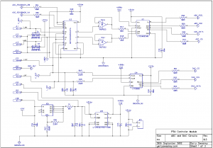
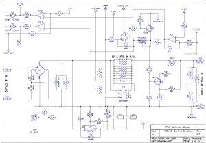
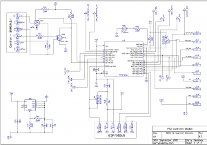
First of all, here is the latest schematic which represents the power supply design as described in this blog and videos with what I believe are the modifications required from the latest round of prototyping and testing.
Here is a video overview of the prototype hardware and test setup as well as some basic tests including load regulation and programmable voltage accuracy benchmarked against a calibrated HP 34401A bench meter.
Here is a video using the software to demonstrate basic set volts, output read-back tests and a benchmark against HP 34401A
I still have the following outstanding issues I want to address before committing effort to laying out a final PCB.
- The “Output Off” circuit needs to be verified to resolve the glitch shown in the video when turning the PSU output on
- Verify remote sense circuit and approach
- Create and test a charge pump to generate a negative supply with a simple regulator, and specifically making sure the diode switching noise does not affect the ADC’s accuracy or stability
- Create a minimum load constant current source for the regulator, and deal with measuring output current and compensating for the current source
- There is currently no output protection of any kind, I need to deal with reverse polarity input (connect a battery the wrong way around to the input terminals), power feedback (connect a battery the right way around and power down the PSU), connect mains AC voltage into the output terminals. Apart from passing thoughts I have not looked at circuit protection at all.
- Verify the accuracy of the current limiting and ADC read-back
In Part 11 I will make further refinements to the design addressing the outstanding items and get a board designed and ordered ready for Part 12 (the final part I hope).
Please do comment and like the videos if you find them interesting. Thank you for watching.
This content is published under the Attribution-Noncommercial-Share Alike 3.0 Unported license.


Gerry,
Couple of thoughts from a very quick read of the current chapter….
A fairly high current diode strapped across the output terminals strapped to not conduct in normal usage but if the battery as you say is strapped accros the output terminals backwards then it will
conduct and prevent more than 1 diode drops worth of reverse polarity being applied to the regulator. a further diode from the live output terminal back to the main bulk smoothing cap that way nothing in the main regulator gets biased the wrong way.
Span
Hi Span, cheers for the suggestions. I think I will also need a polyswitch or other protection device, I don;t know many diodes that can withstand a car battery being discharged into it the wrong way around. The reverse diode back to the smoothing cap would work, in fact there is a diode inside the TIP147. However, because of the design this will have the weird effect of actually powering up the PSU assuming its the correct voltage! I would have to try it and see what happens. Either way I will certainly need have to do something like a crowbar and polyswucth to protect from over-voltage. How I protect it from having mains AC fed into the output terminals is another problem 🙁
Hi Gerry;
I am following with interest your shares and your website.
The previous stored in your schema, choose MCP622 added between 4053 and LTC2402. Why do you need it?
I also fully understand the reason for putting BAS40-04 s. Analog Ground and Digital Ground between the PCB on your (SMD Bead coil) Is there?
thanks
Hi Sadik, the MCP622 is acting as a buffer. The ADC presents a “dynamic current” input which basically means the input voltage is switched into a capacitor at high speed. This creates noise on the input which works its way back through the 4053 into the PSU error amp. The MCP622 buffers this and ensures what comes out of the ADC does not go backwards into the circuit. I am intending to replace the MCP622 with an LT1013 but the purpose is exactly the same.
I do not have any inductors (yet), I don’t believe its needed.
Gerry
Gerry,
I was wondering where you had gotten off to. That darn 9 to 5 thing, huh? It looks like the project has come along nicely. I like the new pass device; simpler to implement than a FET. As you may recall, I am working on a similar project, although mine is all analog.
I am [pleasantly] surprised that you are able to obtain the voltage resolution that you do. I think you have about 200mV of ripple going into the pass device when the load is drawing 1A (Vripple ≈1A ×10mS/4700µF). That means that your regulation circuit is acting very quickly indeed.
Again, great work. All the best,
George
Hi George, yeah that work thing, I love what I do and when I need to get things done it has to take priority. I am much happier with the output stage, the local negative feedback makes such a big difference to the overall stability of the regulator loop. The resolution is really good, well I achieved the same as my HP/Agilent 3136A supply with electronics that are really much smaller and simpler which is what set me out on this path in the first place. The speed of the regulator is really good, I am able to go form off to a surge of over 6A into a 2A load in about 20uS. Unfortunately when removing the load I get a bit of overshoot – not sure what I can do about that, need to play more. I am measuring noise (with 20Mhz bandwidth limit) at less than 10mV which includes all of the environmental and induced stuff, to the best efforts the noise from the PSU is below 1mV which is nice. There is absolutely no 50Hz ripple on the output from what I can measure, even under full load. Still got some work to do though, I am working on the absolute zero output which I how have and am dealing with offsets and current leakages which down in the <1mV range have an impact! All fun though, I am learning loads as I go.
Hi Gerry,
I’ve done a simple spice simulation of the output stage with the help of the ltspice mailing list, just to get an idea of how it will all work. Obviously doesn’t account for a lot of things but might be useful to someone.
https://dl.dropbox.com/u/8513299/psu.zip
Hope to see the next one soon!
Hi Richard,
Thanks for posting the spice simulation. I have not used SPICE very much myself, I probably should use it more. I kinda like building the thing and using the test gear to see whats going on. It will be interesting to see how close the simulation comes to what I actually get. I will mention it in the next blog post.
Gerry
Definitely more fun to play with in real life, I currently don’t really have enough test gear/electronics to test it out but hopefully that’ll change soon.
As an aside, how are you powering everything? It looked from your video like you had a bunch of AC outputs to use?
Hi Richard,
Yes the white box with the 4mm banana jacks on it is simply a couple of toroidal transformers in a box. The box its self is an old X21 router stripped out but conveniently had IEC power connector, fuse, voltage selector etc. just bolted in the transformers and mounted the 4mm jacks and a mains switch. I have two young children so having loose mains around is not an option – safety first 🙂
Gerry
Great power supply project. Probably the best on the internet. Please post updates soon as I can’t wait for more 🙂
Would it be possible to move to better ompamps to compensate for offset? Ignoring the cost of better parts is it possible to get similar performance to what you have with -200mV supply on your circuit?
Hi Johnny,
Thanks for your kind words, I am glad you find the project interesting. I have solved most of the issues now, I have created a really simple split supply using a charge pump and I have made a bunch of other improvements too. The problem is that even single supply rail-to-rail op-amps you can not swing down to zero, at best you are down to a couple of millivolts. Another problem is at the rails, the op amp becomes non-linear too so results are unpredictable. The simple solution is to generate a -Ve supply, from what I can you need to at least 500mV or more. I decided to re-organise the design and run the op-amps at +/-5.5v which is now working really nicely, all still derived from a single AC input circuit.
On the question of better op-amps. The LT1013’s are actually very good, the input offset voltage is about 150uV which is well within the spec I need. The problem I have had though is input offset current, which if not handled can lead to very confusing results – it becomes very relevant when you are measuring down to 1mV resolution at 2mV output!
I will be posting the next instalment very soon.
Gerry
I wanted to design simple modular PSU like yours. Unfortunately I had too little knowledge and measurement gear to design analog part properly and I got stuck at it. I’m amazed at your simple and incredibly precise design. I won’t lie, I’ve shifted my project to be based on your work 🙂
I also want to thank you for your extensive posts and the knowledge you’ve shared. I learned a lot from you.
Hi Johnny,
Glad its of some use. My experience with analog electronics is actually very limited, I am an amateur at this really – although I have learned a great deal more than I knew just by building this project. If you read back through the articles you will see where I have made erroneous assumptions which I have figured out as I have developed the design. Something that started out simple has ended up more complex than I imagined it would become in physical terms but it is precise and works really well from what I can tell. The regulator design is very “classic” and has been done many times over. The output design using a MOSFET as a voltage amp driver with local negative feedback to get low gain for stability is something I have not seen anywhere else (although I cannot imagine its not been done before), that was an inspired moment as I drew an ideal block diagram and realised what I needed was some gain but not too much – the emitter follower needed to be tamed!
I have two more articles by which time I expect to have working modules and a final design leaving me free to do the next part – the front panel controller; the digital stuff and software is a little more aligned with my core skills.
Keep watching and if you do build your own PSU based on this work, let me know, I would love to see it.
Gerry
Hello Gerry, great blog! Following it from start of your project and it is very interesting and informative! Thanks for your knowledge sharing! I’m Interested in why you threw MOSFET from your design and in its place put the BJT and interested in why you threw Preregulator?
Excuse my bad English!
I moved away from the MOSFET to simplify the design of the driver circuit, the BJT is cheap and works well. Same deal with the pre-regulator, that needs some work and I thought I would get V1 finished first and look at the pre-regulator for V2. Thanks for following the project.
Hi Gerry,
First thanks for putting up a great series on modular power supply design. I am planning to prototype my own power supply design with different specs and the protoboard which you are using caught my eyes. Could you please provide me with the details on where you have brought the green protoboard that you are using.
Hi, I bought the prototyping boards on e-bay, search for this “Double Side Prototype PCB FR-4 Stripboard Universal Circuit Board” and you should find some
Gerry