It’s taken me a while since the last update, I have been real busy of late. Having completed the first physical build, I now need to make various changes to the construction. Given the screw-up of the star earthing topology on the first board, I need to layout another board revision so I am going to make a bunch of other improvements. In this article I cover the various design changes and perform some basic power, DC condition and regulator response tests, I identify and resolve some issues and re-select better performing op-amps as an alternative to the LT1013, I have selected the OPA2277U part, and I have also tweaked the power supply implementation for the drive circuitry to reflect the fact that the newly specified op-amp is not a single-supply rated part.
The Schematic
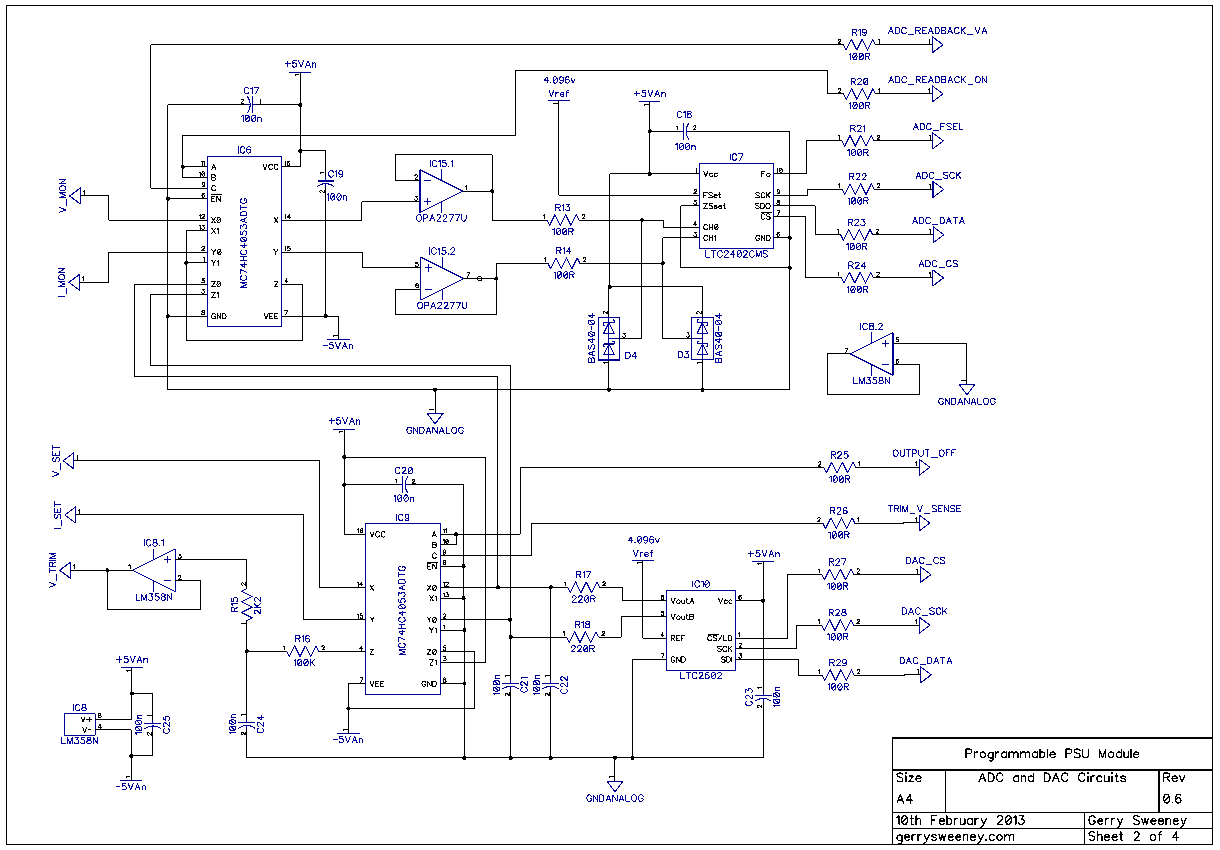
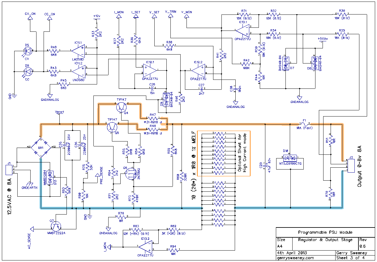
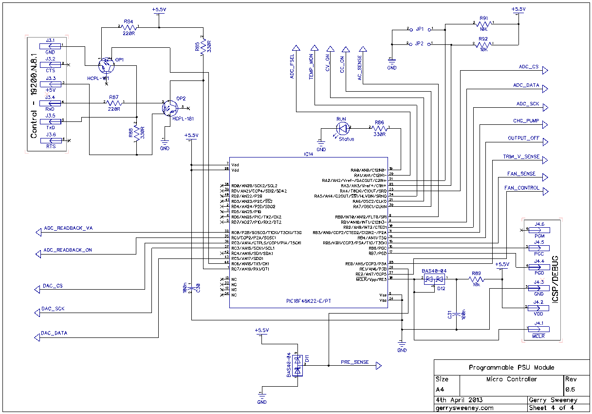
Here are the latest schematic which is at version 0.6 including all of the latest changes.

I now need to test and resolve (or decide its acceptable) the overshoot problem when testing the load/no load dynamic response of regulator. I also need to re-layout the next board revision, get some boards made and build the next version. In Part 14 I am going to cover the firmware, describe the development environment and show the basic software layout as well as details on the current serial protocol I am using to control the module.
Thank you for your continued interest in this project, please give the video a thumbs up if you have found it interesting.
This content is published under the Attribution-Noncommercial-Share Alike 3.0 Unported license.
Nice work. Why you didn’t use variac? It’s provide wide range of supply voltages and currents, but a bit unstable than a toroidal transformer. Also it would be nice if you could to test PSU at a relatively high voltages and currents. Just need to add else 1 or 2 power transistors and check stability of PSU. Or still too early?
I did not use a VARIAC because I don’t have one 🙁 but also because I have young kids so I did not want them “varying” things that might be on a soak test. One of the next jobs is to do the high voltage testing but I wanted to iron out the regulation issues first before I go down that route – so probably a little bit early just yet.
Great work, very informative and practical. and the best part is that you go through design and debugging step by step and explain every detail in the circuit.
thanks very much for sharing
Thanks for the comment. I often worry that I go into too much detail so its nice to hear that I may be a little too self-critical. Thank you for your interest in the project.
Hi Gerry,
Again, nice work here !
At some point you mentioned about shunt resistor, could you be kind to tell us more info about that? You said something about Switzerland… Nicrom Electronics it’s the one, or SRT, or another one ? I’ve seen that Vishay makes a lot of those, but I think those are expensive…
I’m looking forward to see your next part 🙂
Cheers,
Nicu.
Hi, this was pointed out to me by one of the followers of the project: https://www.elfa.se/elfa3~tr_en/elfa/init.do?item=60-575-44&toc=20042 I have some on order. The supplier is called ELFA who are a distributor.
Hi,
First .. excuse me for my lack of understanding. But isn’t it a problem mounting the sense resistor on the heatsink?
The heat generated by the pass transistors will cause the resistance to rise, hence the current measurement will be off at high loads… Or am I missing something??
BR Jonas
Hi Jonas, yes thats true but at 8A the resistor gets very hot because it dissipates about 6.5 watts so it needs to be cooled to a reasonable level, I will almost certainly be able to compensate in software as any temperature related errors should be linear and in direct proportion to the temperature of the resistor. The tc of the resistor is quite low at +/-30ppm/degreeC so I am not expecting too much of an error, it will certainly be better than the free-stadning situation where I may well end up with a component failure. Perhaps on the low current version the resistor could be not mounted and left floating, not sure I would need to test how much of a problem it would be.
Very interesting project, and I like the mechanical layout of your module. Thanks for posting on the blog and YouTube.
Regarding that you found the raw voltage insufficient for 8 V, 8 A output in your video however, I’d suggest you check the current draw from the transformer with a true-RMS showing meter before you just increase the output voltage. In your schematic you have indicated a 12.5V AC / 8 A input, but at an output current of 8 A, the input RMS current will be considerably higher than 8 A. Depending on transformer impedance, it will be roughly in the range of 1.5 to 2 times the output DC current. (The rectified-average of the input current will however be 8 A, as one might expect)
You might also want to consider whether you need to support maximum output current and voltage at low line voltage. From what I have understood, the whole of EU has 230 V +- 10% nowadays (207 V – 253 V).
Very good points, I did consider the variation in line voltage which is why I upped the RMS voltage higher than I should theoretically needed. I need to get myself a VARIAC and do some testing one day 🙂 I will make a point of measuring the RMS current drawn on the AC side, I would expect you are right, I can probably establish the expected current by looking at the power dissipated in the load + the power dissipated in the regulator should equal the power being drawn from the winding, not sure it would be double but it will certainly be more than the DC output current. A nice practical solution is to soak test the 8A rated transformer for 24 hours and see if the transformer gets hot and bothered, I suspect it would be OK.
It is true that the active power drawn from the transformer would be like that – conservation of energy and all that, but the problem in this case is that the current waveshape is not sinusoidal. So power factor ends up being less than unity, not because of phase shift but because of harmonic currents.
For an example of what it can look like, see Table 1 here (not my page):
http://sound.westhost.com/power-supplies.htm#ripple-current
Even though the AC current may be up to 2 times the DC current, this doesn’t mean the power factor is as bad as 0.5 however, because the DC voltage on the output side of the rectifier is still higher than the transformer RMS voltage.
I and a friend used a 2x 20 V 6 A toroidal transformer some time ago to build a dual laboratory supply. We did however use floating supplies for the control circuitry like many of the Agilent supplies use, and did this by hand-winding, for each channel, a 15-0-15V winding onto the toroidal transformer. It was a little messy but worked out fine.
By using a triac the rectifier can be switched between a normal configuration and a voltage doubler. In doubler mode we can reach 40 V, and at 1.5 A DC output the transformer current was verified to be 6 A RMS, like we had previously simulated using measured resistance and leakage inductance of the transformer. In normal rectifier mode 6 A RMS from the transformer was reached at 3 A DC output current. We could reach about 20 V output, with the effective smoothing capacitance being 7000 µF.
You make some good points, I will do some measurement around this and see what I get. I am waiting for the right current shunt resistor so I can run the PSU at 8A safely over an extended period of time which will allow me to make some decent measurements. At the moment, 8A is likely to smoke my current shunt resistors. Thanks for posting the link to the power-supplies document, looks really useful. Gerry
Hello Gerry, you might like to steal (and i am sure they didn’t invnet it) a temperature monitoring trick from Maynuo.
Inside, you will find a rediculously overrated bridge rectifier, which has the phyiscal/mechanical adantage of being bolted directly to the heatsink. Disregard the two AC legs and you are left with a pair (well, two pairs, but that’s irrellavent) of forward biased silicon diodes between the – and + terminals, that will exhibit a voltage drop of around -4mV/C.
Cheap, too! This would do the job http://uk.farnell.com/multicomp/vsib410/bridge-rectifier-4a-100v-gsib-5s/dp/1861531
Hi Lawrence, yes thats a very good suggestion and as you say its cheap too, cheaper than the TO220 device I was looking at. Thanks for the pointer – I do have a spare LM358 op=amp element in the current design too -lovely.
Great work !!
This project is really interesting, I’d be interested if you make a kit or partial kit out of this.
I really like the way you have described the development process, a lot of things to learn from this.
Glad you have found it interesting, thank you for reading/watching. I am not sure if I would be able to make a kit, I will most likely make a decent quantity of PCB’s once the final design is done to make those available to people that might want one. Gerry
Ok, I’ll probably be in for a couple of PCB’s if that’s what’s going to be available.
Anyway, I got a few questions.
First, what does the modification to the transformer do with the VA ratings of the transformer?
If you have a 10V*8A (80VA) and changes this to 12,5V you should have only 6.4A available since 12.5V*6.4A=80VA, and 12.5V*8A=100VA.
Correct?
Second, I see that your schematic is ground referenced on the input side of the sense resistor. What happens if one connect a scope that’s ground referenced to a circuit connected to the output? As far as I can see this will “short” the sense resistor via the mains ground.
The VA rating of the transformer is dictated by the core size and the primary winding. For my purposes, the transformer has been wound to support three channels totalling 260W and its highly unlikely that all three channels will ever all be run at full load for extended periods of time. The power requirements remain the same and subject to there being a reasonable power efficiency between AC in and DC out of the regulator then it should remain within tolerance – at least for what I am trying to do with it.
You need to be aware of the low-size current sensing topology when you are scoping around. However, the PSU is fully mains isolated so using a single scoping point anywhere on the circuit will on interfere with its operation.
Ok, thanks.
So the total power drawn from the transformer is within the specifications.
Guess I’m just being overly paranoid here. 🙂
I’ve had a transformer getting way to hot on me before, not a pleasant experience.
Fantastic stuff! I have enjoyed every one of your videos.. and the level of detail is perfect. I wouldn’t change a thing. I would love to build one of these… all I have is a crusty Trygon single power supply from the 70’s that leaves a lot to be desired! Looking forward to the next video Gerry.
Dave
Hi Dave, thanks for your comments and thank you for watching the videos. iam working on Part 14, should be done soon. Gerry
Hi Gerry.
Thanks for putting so much effort in to sharing your project. I learned a lot and was inspired both by you and Dave on EEVBLOG to build my own design
Did you ever look at output noise? If so, who did you go about it and what did you achieve?
My objective was to get to 5mV output resolution. Even with the usual decoupling and layout precautions I am measuring ~+/-8mV of noise (to 3 standard deviations) on the output. So, if I specify 1% max noise on the output, that means my real resolution is 800mV?
I based my PSU around an STM32F100 MCU (Cortex M3). I thought this was a nice device because it integrates 12-bit A-D and D-As. (I think the dual independent D-As is a unique feature?) The second DA channel is really useful as a digital trimmer. At $3.84 in 1-off qtys I think it’s a cheaper way to go than buying discrete MCU, AD and DA. In addition, with PCB at ~$5/sq inch for 3, integration saves board area. Out of interest, how much can you get 2 layer PCBs for?
Your article about MCU toolchains resonated, especially if you add in the (unnecessary!) complication of using a Mac as your development platform….. Since the F100 is an ARM device, toolchains can get expensive. In the end I spent time building GNU tools under Eclipse which was an interesting learning experience in itself…
Best. Liam.
Hi Liam,
Thanks for the comments and feedback, I am glad you like the project. Noise – yes I spent some time looking at that, the noise is down in the weeds around ~5mv measured on the scope, but much of that noise is environmental rather than from the supply specifically. Benchmarked against one of my Agilent PSU under similar conditions the module is every bit as good, perhaps even a little better with regards to noise performance.
I started with 12bit ADC/DAC but effective resolution was not good, the INL and DNL was just too much to bear, in the end I am using a 16-bit DAC and 24-bit ADC which for the project seems about right and meets the design goal of 1mv resolution.
2 layer boards I got 5-off for about $60 for the size of the module.
Yeah ARM tools are expensive 🙂 thats probably what stops me from switching to ARM from Microchip
Gerry
Gerry