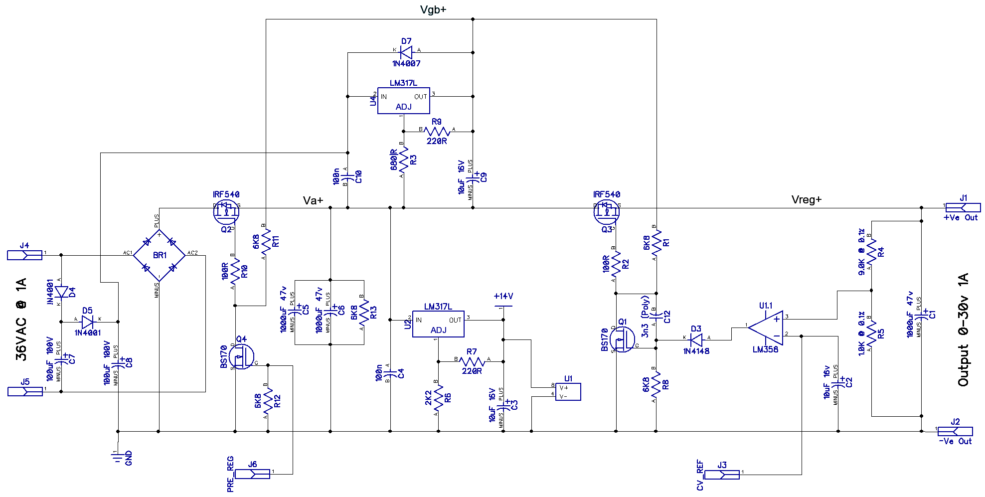
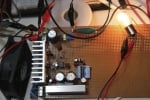
Previously in Part 2 I created a simple regulator circuit using a pass device and an op-amp, I was basically putting the well understood theory of this kind of circuit into a practical circuit and verifying my own basic understanding. Apart from no-load DC conditions which were fine and dandy, any sort of even moderate resistive or capacitive load drove the circuit into wild instability, clearly the breadboard its self, thin connecting wires and long component leads as well as a lack of any star earthling were all going to contribute to this, so it was time to refine the circuit a bit and build it on a more sturdy vero board with some attention to layout, earthing and current handling. Here is the circuit I built: –
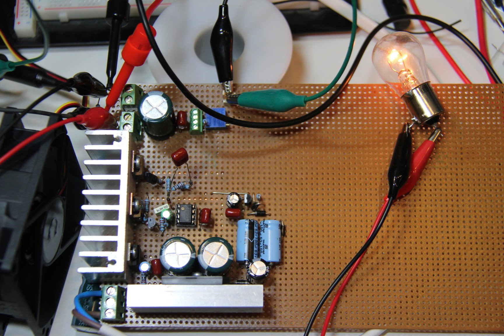
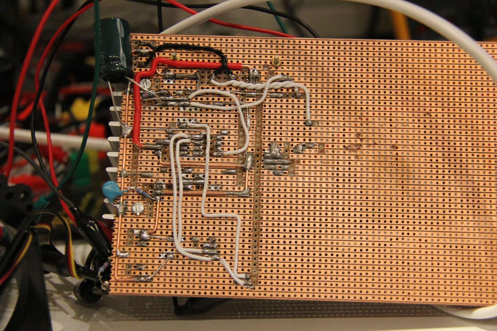
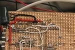
The initial prototype is a throw-away, that means I build it on vero (strip) board, use low/no cost components, cheap sockets for the IC’s I want to re-use and as many components as possible from the junk bin – when I am done with my testing I strip anything worth keeping for the next project and throw it in the bin – the point is, don’t expect it to be pretty…..
The significant change was adding gain to the circuit which is critical if I am to get the desired output range of 0-30 volts. The gain is obtained in Q1 which is in the classic emitter follower (if it was a NPN BPT) configuration. Having this configuration for the driver means I only need a swing of between 1 and 2v to get the full output swing of 0-30v. Needing a small voltage swing means I can run the op-amp at 14v. The driver and output is acting as a voltage amplifier which is what FET’s are good at doing. The diode D3 is ensuring that the op amp is running in class A in the required range driving into R8 which is its load. By doing this we eliminate any potential crossover distortion the op amp might exhibit because of its internal center point.
The op-amp U1.1 is doing the error correction. The driver FET (Q1) is inverting, which means the negative feedback from the output of the regulator is actually fed into the positive input of the op amp, this is a different configuration to the first design where the driver was a current amplifier and non-inverting.
One interesting addition is the Vgb+ supply voltage. You will see that I have included pre-regulator pass device (Q2), the idea here being when there is a large amount of power being dissipated across Q3 the micro controller can detect this and drive Q3 which in conjunction with C5 and C6 will act as a bucket style pre-regulator. Because Q3 is acting purely as a switch we need it to be both very fast and very low on resistance and one of the things a power FET does very well is have very low on resistance. However, in order to get this low on resistance, you need to drive the FET’s gate pin at approximately +5v above the source pin. That means if you have 30v on the drain, and you want to see 30 volts on the source, then you need to drive the gate with +35 volts. Vgb+ is obtained by using a simple AC voltage doubler and a series regulator that’s referenced from +5, giving 5v above V+ regardless of input voltage.
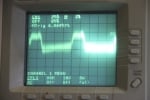
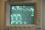
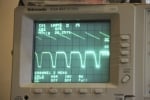
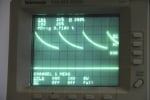
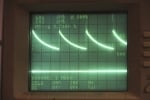
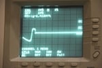
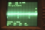
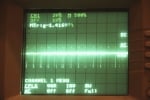
So filled with high expectations I power up my new masterpiece for the first time and err, well not great. Unstable is an understatement, I had high frequency instability, low frequency instability and wildly different variations of the same with different loads. For the most part, a large electrolytic cap across the output brought it mostly under control, the high frequency stuff was largely killed off by placing C12 on the driver (Q1). Various loads across the range would yield different results and it was unpredictable and certainly not reliable in a way that I would be happy to power my next project from it!
So whats going on? why are these types of circuits so unstable? Well, I am sure there are very detailed scientific explanations but I don’t have anything like the knowledge to explain those; so in layman’s terms this is the best I can do. Under perfect DC conditions, the ideal circuit (which is how I tend to visualise electronic circuits) there is negative feedback and no phase shifts so you have a perfect DC Servo, so it locks the output to the input reference and as load is placed on the output the error amp drivers more or less to maintain the output at the input level – easy right? Unfortunately, all electronic components, wires, board layouts power sources and environments generate noise and have parasitic inductance and capacitance all of which can introduce phase shifts at different frequencies – this means that across a frequency spectrum our perfect theoretical circuit with its perfect negative feedback actually turns into positive feedback and your stable DC servo becomes an oscillator, your circuit can be stable at one frequency and totally unstable at another frequency and this can be occurring at the same time. Worst case you have numerous different stable and unstable conditions concurrently.
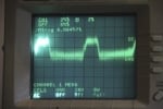
As I was measuring this behaviour I was observing a lot of fluctuation, things were varying in a random and unclean way, the analogue equivalent of a random number generator in software. To me the circuit felt very loose and reminded me a lot of those old fashioned black and white CRT TV’s I used to play with when I was a kid, The whole thing was powered by a big dropper resistor and change in the percentage of white/black proportion would significantly change the voltage levels in the TV’s electronics and this could be seen visually as instability as the picture would appear to breath and move around on the screen as things changes. Compare that to later solid state CRT TV’s where regulated power supplies were used, everything was much more stable visually.
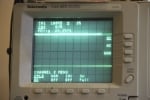
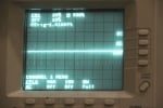
I had managed to quieten the PSU down and drive into loads with good regulation and I achieved this by slugging the think with capacitance which has the effect of lowering the bandwidth of the circuit, which means the circuit has no, or substantially reduced gain at higher frequencies and any oscillations at those frequencies obviously go away. The problem with reducing bandwidth though is the impact on the dynamic response of the PSU under varying load conditions (more on that in a future article).
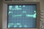
Types of capacitor also play a big part, for example I was only able to stabilise the high frequency issue using a 3n3 to 10n polyester cop, putting in the same value in multilayer ceramic did not work – that was yet another indicator that the circuit is simply too sensitive to instability – its loose.
My test conditions were done mainly under a 5-10 watt load at about 15v. I have attached some photos and some scope traces so you can see the sort of effects I was seeing.

In summary, despite having it quiet and stable with various test conditions I was left with the impression that the circuit felt wrong. At this point I am suspecting many things, the FET’s are very fast so they were a concern, the feedback loop is running at high power levels so effects of parasitic capacitance and inductance are very pronounced. My overall take away was I need to start again and just for a while I thought, maybe I should just use an off-the-shelf IC solution – but I felt like I was giving up to easy. I don’t have the skills and experience to design this scientifically so I have to approach this with a bit of trial and error and a lot of instinctive sauce. That desire to not give up got me thinking – and an idea came to me – what if I created a very low-power regulator which was highly stable at the desired voltage range and then scaled that up with a simple current amp – could I get better results?
In Part 4 I will share with you the great progress I made and a fully working regulator design.
This content is published under the Attribution-Noncommercial-Share Alike 3.0 Unported license.
Think of what happens when this supply is used, for example, to charge a small lead-acid battery and you turn the power off. There are unfortunately plenty of commercial power supplies, including some from HP, that go “poof” in such circumstances. A partial solution is a diode in series with the output, perhaps with an ideal diode controller to cut losses. Linear has ideal diode controller(s), other must too, I’d think. Your limited schematic doesn’t imply a problem, but once you add, for example, an overvoltage protection crowbar, you’d get a nice self-destruct mechanism for the supply if you don’t have that diode. I’m not sure either how well would your design would survive right now now being back-driven with a negative voltage. The series diode will conduct if you attach a negative voltage source, and a lead-acid battery or even a small laptop-style rechargeable battery has low enough impedance to liberate magic smoke unless you explicitly engineer protection and/or build in tolerance for such common situations.
I’d say that a reasonable design goal must be to survive indefinitely connection of ideal (zero impedance) voltage source producing anywhere between zero to 150% of rated output voltage in either polarity.
Hi Kuba, yes you are correct, there is no effort on my part at this stage to provide any protection outside of short circuit protection (current limiting inherent in the design). My plan was to get a working PSU and then focus on protection really as a separate exercise. You will see that the pass device actually has an integral reverse diode across it’s drain/source so any correct polarity feed in will be passed back to the reservoir caps; in the voltage range of the device and caps pass device should be protected. Instinctively, I would not want to put a diode in series with the output because that will dissipate power at the higher currents. My feeling is a fast high power diode strapped across the output for reverse feed-in protection and a fast crowbar for over voltage protection (which would also deal with correct polarity feed in) and to protect the crowbar and reverse diode either a fuse or resettable trip/breaker arrangement. I agree that the PSU must be able to withstand some reverse and forward feed in, and there needs to be something fusible to protect the protection circuitry, and that will certainly be the subject of at least one of the posts in the series.
As I’ve said, a diode won’t protect you if you attach a negative voltage source. The current will be flowing *out*, but various parts that are attached to the output will suddenly see a negative voltage, and they may not like that.
I’ve also mentioned an ideal diode controllers, such as . Those turn a mosfet into an ideal diode that dissipates no power at all.
The part I mentioned was http://www.linear.com/product/LTC4357.
Hi Kuba, I diode strapped across the output in reverse would deal with reverse polarity feed-in – assuming I have some kind of thermal cutout or fuse. I can not use an ideal diode here because the FET (or by the looks of it this ID controller) would not survive the reverse voltage. I have never come across the ideal diodes before they look interesting for power switching, all of a sudden it have become clear how N+1 PSU’s can be placed in parallel and switch over.
Thanks for the comments/suggestions