Fully Programmable Modular Bench Power Supply – Part 7

Now I have the requirements for the control ranges I need its time to get down to the nitty-gritty and get a DAC up and running so we can make some measurements. The maximum dynamic range I need for this project is 6000 individual steps – this was identified in the calculations for the voltage control for the 0-6V rage in Part 5, so let us start there.

There are many options for DAC’s to choose from, I want to keep the cost and component count down so my starting point is a low-cost single component solution from Microchip, part number MCP4822. This is a dual 12-bit DAC with two channels and a built-in voltage reference. I get independent voltage and current control from one 8-pin chip – wow! However, there is a problem with this part, it only has 12-bit resolution which will only give me 4096 individual steps and my design calls for 6000. The problem with choosing components with a higher number of bits is that they start to get expensive. I want to see if it’s possible to extend the range of the DAC using software and a technique called “dithering” or “modulation”.

The idea here is pretty simple, to increase the resolution of the DAC you can continuously switch the output between two or more codes, feed the result into a low-pass filter and get the average voltage. If you switch between two adjacent codes with a variable mark space ratio like you do in PWM, it should be possible to extend the range of the DAC without creating large ripples on the voltage head making the low pass filter easy to construct. That is the theory at least, I need to try it and see what the results are in practice.

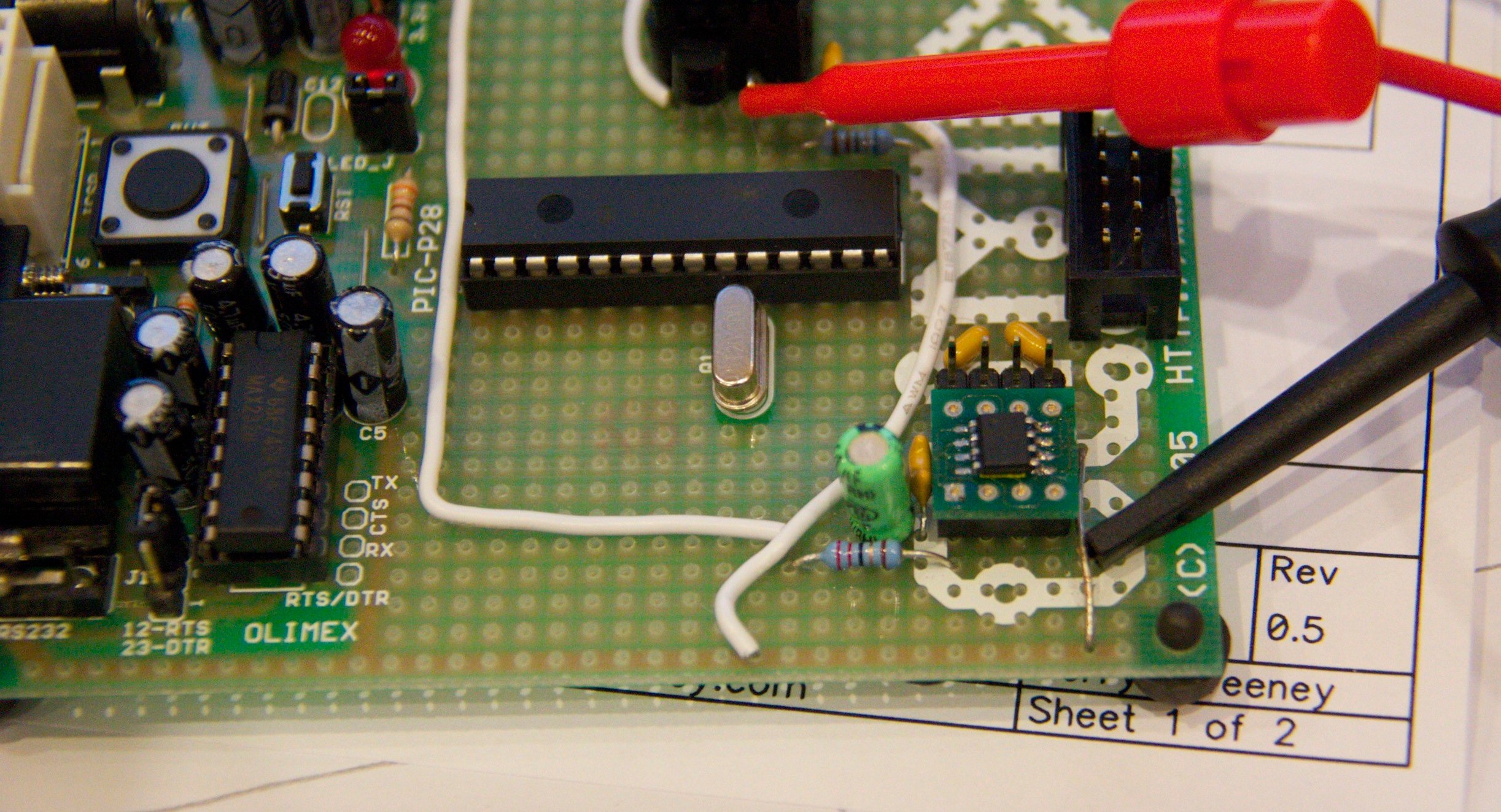
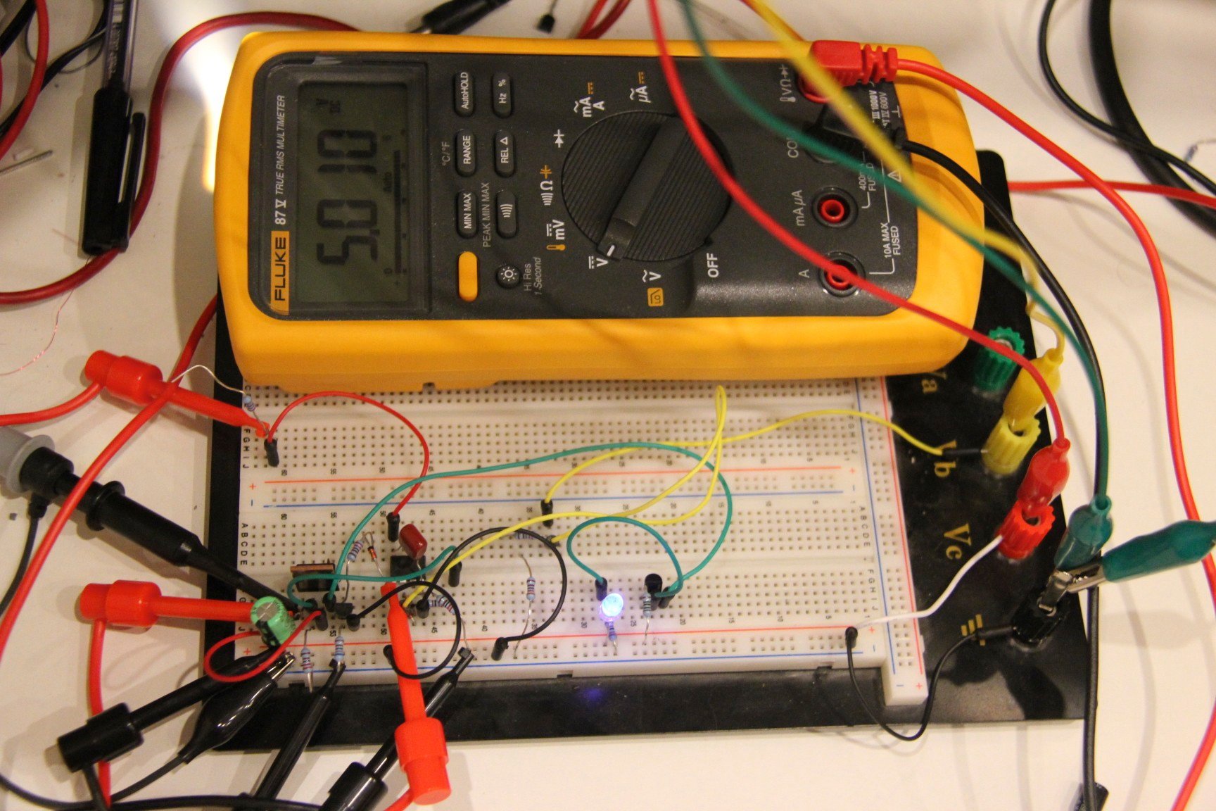
Before getting too complicated though, I thought it would be good to run the DAC in static mode, set some codes and measure what we get. The DAC has 4096 steps, the internal reference voltage is 2.048v and the chip has a x2 gain option so I should be able to program any voltage between 0v and 4.096v in 1mV steps by simply programming a digital code between 0 and 4096 into the DAC channel. To get this up and running I hooked up a PIC micro controller, the DAC chip and an RS232 serial interface. The firmware in the PIC will allow me to interact with the DAC through a simple serial terminal on my computer.

Before any MPS430, Atmel or Arduino die-hard fans start giving me advice on micro controller choice — forget it. They are all good parts, I just happen to personally like PIC’s because I know them and I have the tools and a whole bunch of them sitting here to play with – if you are not happy with my choice of micro controller thats tough…. I am not going to change it or enter into any debate over the pro’s and cons of other devices – I am sticking with PIC’s for this one and if you try to change my mind I will ignore you – sorry.

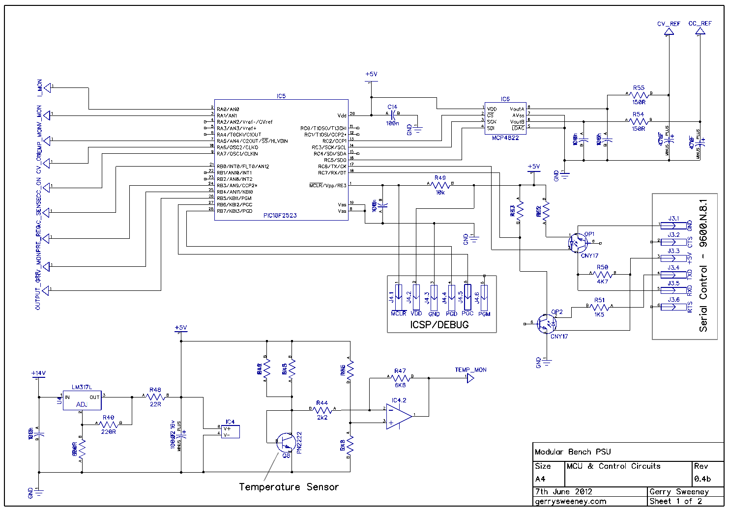
Here is the schematic diagram for the prototype I am using.

For the dithering I have decided to extend the DAC by 2 bits. Extending by two bits means I have to write a sequence of four codes continuously in succession to the DAC. I am writing approximately 1000 codes per second within a timer driven high-priority interrupt routine which ensures that the timing remains constant. Timing errors will introduce more DNL errors so the code stream needs to be constant and accurate. The codes written are the base code value followed by the base code value + 1. The two least significant bits from the now 14-bit word controls how many times each of the two values is written. For example, to get four steps between code 100 and code 101 we would write the following codes: –

100.00       100   100   100   100
100.25       100   100   100   101
100.5        100   100   101   101
100.75       100   101   101   101

Extending by 3 bits is an option and would mean I have to write a sequence of eight codes, again following the same explanation as above, here are the codes that would be written

100.00        100   100   100   100   100   100   100   100
100.125       100   100   100   100   100   100   100   101
100.250       100   100   100   100   100   100   101   101
100.375       100   100   100   100   100   101   101   101
100.500       100   100   100   100   101   101   101   101
100.625       100   100   100   101   101   101   101   101
100.750       100   100   101   101   101   101   101   101
100.875       100   101   101   101   101   101   101   101

I tried the three bits as an academic exercise but I have decided not to go to three bits because of the noise, ripple and integral errors generated. The cost of the filter circuitry and the expansion of the line items in the bill of materials would probably outweigh the cost of upgrading the DAC component to a higher resolution part.

I have selected a number of spot voltages in the range to benchmark what I get from the DAC. The following table sets out the results I measured. (I am using a calibrated HP 34401A meter for all measurements).

Spot Voltage DAC Code Measured
MCP4822
(12bit static)
Error DAC Code Measured
MCP4822
(14bit dith)
Error
0 0 0.0015V +0.0015V 0 0.0014V +0.0014V
0.001V 1 0.0015V +0.0015V 4 0.0016V +0.0002V
0.002V 2 0.0024V +0.0014V 8 0.0026V +0.0006V
0.003V 3 0.0034V +0.0004V 12 0.0036V +0.0006V
0.004V 4 0.0044V +0.0004V 16 0.0046V +0.0006V
100mv 100 0.1024V +0.0024V 400 0.1026V +0.0026V
500mv 500 0.5024v +0.0024 2000 0.5026V +0.0026V
501mv 501 0.5034v +0.0024 2004 0.5036V +0.0026V
1V 1000 1.0004V +0.0004V 4000 1.0006V +0.0006V
1.5V 1500 1.4975 -0.0025 6000 1.4977V -0.0023V
2.5V 2500 2.5014 +0.0014 10000 2.5016V +0.0016V
3V 3000 2.9993 -0.0007 12000 2.9995V -0.0005V
3.001V 3001 3.0002 +0.0002 12004 3.0005V +0.0005V
3.002V 3002 3.0012 -0.0008 12008 3.0014V +0.0006V
3.9v 3900 3.8968 -0.0032 15600 3.8969V -0.0031V
4.095v 4095 4.0916 -0.0034 16379 4.0916V -0.0034V

Well, that is disappointing given I am aiming for a precision of 1mV and to get a control voltage of 0-6V I need accurate 500µV steps. So whats wrong here? Having read the data sheet there are some gotcha’s that naively you might ignore as I did. Every DAC has two really important parameters called Integral Non-linearity (INL) and Differential Non-Linearity (DNL). The DNL defines the maximum deviation to expect from the “ideal” voltage for any given code, expressed in LSB’s (or counts from ideal) and INL is the accumulated DNL errors that occur over the whole range. Fundamentally, the DAC is based on a resistor string network and its not easy to make highly accurate resistors, as soon as you start needing more accuracy the cost of the part rises very steeply, and even with the best part money can buy there will still be errors. The more bits you extend the DAC by using dithering, the more error you introduce and the more noise you introduce too. While extending by two bits is probably acceptable with a decent low-pass filter, extending by three bits and beyond is not really practical. As an aside, the noise figures for the MCP4x22 parts are not that great – something one must consider when the reference voltage generated is going to be amplified, the noise will also be amplified.

In summary then, I want accuracy and precision but I want reasonable cost and even if I spend a lot of money I will still have errors. The lesson learned for me is I now no longer think of a DAC as an accurate programmable voltage source – it’s not, it is a close approximation only. The MCP4922 (MCP4822) is a nice part for the $$$ and useful for some things I have no doubt, but it’s not good enough for what I want to achieve in this project. Even with the resolution extension to 14-bits it falls short. Actually to be fair, even with the errors in the DAC this would be make a pretty good degree of control, it is probably more accurate than most of the lower end bench PSU’s out there, but my benchmark is the Agilent E3631A so I need to achieve much better than this. The MCP4x22 device is the best resolution DAC Microchip do so I must now search for other parts instead – Linear Technologies and Analog Devices are the logical starting point for my search.

There is one further possibility which I have yet to try, which is to combine both 12-bit DAC outputs to create a much higher resolution DAC, the block diagram for such a solution is shown in the data sheet for the part. This is well worth a look because if it works well enough, the cost of the two chips may well still be cheaper than an upgraded DAC part. I will build this out at some point and give it a try.

This project also needs to implement metering in order to monitor the output volts and current drawn by the load connected to the PSU, and this needs to be reasonably accurate to 1mV too, that’s 5-digits I need which in its self is a tall order. However, it occurred to me that if I could get an ADC that was accurate enough and a DAC with enough resolution to provide headroom for trimming it might be possible to build a self-calibrating system that trims the DAC output to match the desired programmed voltage each time you set a new voltage. That is what I will look at in Part 8.

Fully Programmable Modular Bench Power Supply – Part 1

After fixing a high quality power supply (see here if you are interested) it spurred me on to have a go at designing and making my own – I think anyone who does electronics as a hobby will at some point or another build a power supply to use on their bench – I have not done that myself before so I thought I would give it a go. My aim is to use my basic understanding of analogue electronics and create a fully programmable bench PSU that will perform at least as well as the Agilent PSU, I think this aim is reasonable on the basis that todays components are considerably better than those that were available 20 years ago. Apart from the performance characteristics, there are a system engineering characteristics that I also want to consider because I would like to make it possible for anyone else to build this PSU as a DIY project with the ultimate aim of creating a high quality PSU that is modular and can be built in various configurations and be built at a hobby user or small lab price point. Here is a photo showing the very first working prototype regulating at 5.010 volts.

The first working prototype regulator

Why a PSU project, there are hundreds of them already? Firstly, the two areas of technology I really enjoy are electronics/embedded and software development and this project requires a fair amount of both to be brought together. Apart from that, no other reason than because I think I can do a decent job – we shall see 🙂

I thought it would be a good idea to try and set out what I have in mind. My aim is to create a modular PSU system designed to be used in lab or test automation environments. The first thing I want to create is a module similar in concept to those audio amplifier modules you can buy for building a HIFI amplifier, the module will physically look something like this.

The PSU module will take a single AC input from your line transformer of choice on its input and will provide a fully programmable lab quality Constant Current/Constant Voltage regulated DC output. The module its self will not have any kind of controls or display, but instead will have a fully isolated serial I/O which will be connected to a controller with the idea being you can create a multi-channel PSU with isolated outputs while also providing a single earth referenced controller that can be safely connected to a computer or other test equipment in test automation environments. Once I have created these modules, my intention will be to make a a few variants of controller, an RS232 interface and a PC software controller, a simple stand-alone control board with an LCD display and a couple of rotary encoders to control a single module and a more comprehensive control board that can control up to four modules with a nicer display (TFT/VFD?) and other interfaces such as RS232, USB and Ethernet to create a full function standalone multi output bench PSU.

Focusing back on the PSU module, I would like it to support a number of configurations with just a few component changes, primarily this is to allow different voltage/current ranges and resolutions to be selected to suit different requirements.

The headline specs for the regulator module are as follows: –

  • Up to 50w of power
  • Output range options 0-6vdc 0-5A, 0-10vdc 0-5A, 0-15vdc 0-2.5A, 0-25vdc 0-1A, 0-30vdc 0-1A
  • Constant Voltage and Constant Current capable
  • Remote sense capability
  • Over voltage, over current, reverse power and short circuit protection at all power levels
  • Optional on-board pre-regulator to lower the modules heat dissipation for higher voltage ranges
  • On-board temperature monitoring
  • Fully isolated serial interface for programming, control and monitoring
  • Control resolution down to 1mV and 1mA in low voltage range

There are also some system engineering constraints I want to apply, these are: –

  • Low component count
  • Easy to source low cost components
  • Easy to build DIY
  • Physically robust construction
  • One single PCB design for all voltage range configurations

In terms of my design approach, and I must state at this point that I am no analog electronics expert, I really just have a passing understanding. None the less, I want to avoid using the easy option in the form of the classic single package regulator IC’s that most DIY PSU builders use. LM317T, LT3080 and the like. These are great components, don’t get me wrong, but what you don’t get with these is a professional grade PSU without putting a significant amount of other electronics around them, by which time you have pretty much lost any advantage you have gained over using discrete components. Apart from that, one of the main drivers for this project is to learn more about building this kind of project and to share that learning with others.

In Part 2 I will describe my first attempt at building a discrete linear voltage regulator, with a schematic of the first working circuit along with a description of what I found along the way.

HP/Agilent E3631A Power Supply Teardown & Repair

I recently bought a faulty Agilent E3631A bench power supply on e-bay which I thought would be a nice addition to my *slightly excessive* electronics hobby workbench.  These power supplies are really nice; they are engineered and built like military equipment, good high quality materials and mechanically very robust.  An great indication of how good these things are is the second hand values, these things cost $900-$1000 to buy in reasonable condition so they are not cheap.  I bought this particular one faulty and thought I would have a go at repairing it.

My first impression of the electronics in side was not great, it seemed very seriously over engineered for what it was trying to achieve.  It seemed like the designers had a field day adding all sorts of crazy circuits because they could.  The ADC is made up of discrete IC’s, there is a custom logic chip in there as well as a CPU, ROM and RAM, there are numerous power supplies for bias and control circuits all floating around each other and most things seemed much more complicated than they need to be.  The one real surprise though was the opto isolation in the analogue domain. The CV and CC reference signals from the DAC for the +6v supply are isolated through high linearity opto couplers type HCNR200, this is something that would be crazy to do today when the cost of micro-controllers are so low and have all the goodies like DAC’ ADC’s and PWM’s making isolation in the digital domain a far more sensible design choice.

6vIsolation

In fairness though, I was making my initial judgements based on what’s possible with today’s components, things were very different 20 years ago so given its age it’s a pretty sophisticated piece of kit really.  Once working it does appear to work very well so my initial thoughts are not really founded on anything other than my own instinct to want things to be easier to understand and better as a result.

On with the repair….

First things first, after a quick check of the obvious big components like the series regulator transistors etc, I very quickly needed a schematic diagram. Agilent were less that helpful here, the manuals they put out now days specifically have the detailed schematics removed from the documents despite there being a reference to them in the index. When I contacted Agilent and asked for a schematic I was told in no uncertain terms (after a 4 day response time) that they no longer make the schematics available, but they do offer a £450 exchange repair service – come on HP/Agilent, by all means offer the service but don’t stop those of us who want to hack around from doing so.  The solution was to buy an original printed service manual which did include the schematics; e-bay and $10 got me what I needed.  As luck would have it, while waiting for the manuals to arrive in the post, I also managed to find a manual on the net which still had the schematics present – not from any official Agilent source I might add…

I set out to work on fixing it and found I had to strip it down completely, removing the two boards, front panel, transformer and wiring from the chassis and spread it out on the bench. If you find yourself needing to repair one of these, be prepared to commit serious bench space to the exercise.  I have taken a bunch of photo’s if the teardown so you can see what all the bits look like.

Home » HP/Agilent E3631A Power Supply Teardown & Repair » HP/Agilent E3631A Power Supply Teardown
IMG_4987.jpg
IMG_4987.jpg
IMG_4988.jpg
IMG_4988.jpg
IMG_4989.jpg
IMG_4989.jpg
IMG_4990.jpg
IMG_4990.jpg
IMG_4991.jpg
IMG_4991.jpg
IMG_4992.jpg
IMG_4992.jpg
IMG_4993.jpg
IMG_4993.jpg
IMG_4994.jpg
IMG_4994.jpg
IMG_4995.jpg
IMG_4995.jpg
IMG_4996.jpg
IMG_4996.jpg
IMG_4997.jpg
IMG_4997.jpg
IMG_4998.jpg
IMG_4998.jpg
IMG_4999.jpg
IMG_4999.jpg
IMG_5000.jpg
IMG_5000.jpg
IMG_5001.jpg
IMG_5001.jpg
IMG_5002.jpg
IMG_5002.jpg
IMG_5003.jpg
IMG_5003.jpg
IMG_5004.jpg
IMG_5004.jpg
IMG_5005.jpg
IMG_5005.jpg
IMG_5006.jpg
IMG_5006.jpg
IMG_5007.jpg
IMG_5007.jpg
IMG_5008.jpg
IMG_5008.jpg
IMG_5009.jpg
IMG_5009.jpg
IMG_5010.jpg
IMG_5010.jpg
IMG_5011.jpg
IMG_5011.jpg
IMG_5012.jpg
IMG_5012.jpg
IMG_5013.jpg
IMG_5013.jpg
IMG_5014.jpg
IMG_5014.jpg
IMG_5015.jpg
IMG_5015.jpg
IMG_5016.jpg
IMG_5016.jpg
IMG_5017.jpg
IMG_5017.jpg
IMG_5018.jpg
IMG_5018.jpg
IMG_5019.jpg
IMG_5019.jpg
IMG_5020.jpg
IMG_5020.jpg
IMG_5021.jpg
IMG_5021.jpg
IMG_5022.jpg
IMG_5022.jpg
IMG_5023.jpg
IMG_5023.jpg
IMG_5024.jpg
IMG_5024.jpg
IMG_5025.jpg
IMG_5025.jpg
IMG_5026.jpg
IMG_5026.jpg
IMG_5027.jpg
IMG_5027.jpg
IMG_5028.jpg
IMG_5028.jpg
IMG_5029.jpg
IMG_5029.jpg
IMG_5030.jpg
IMG_5030.jpg
IMG_5031.jpg
IMG_5031.jpg
IMG_5033.jpg
IMG_5033.jpg

There were various faults with the PSU, numerous op amps and some CMOS logic IC’s were faulty as well as two open circuit 33k resistors. At a guess I would say there was some kind of big static or high voltage discharge into or across the outputs that caused the original fault. I had to isolate the various areas of the circuit and work on them individually, making assumptions about what should be present in terms of voltage levels and feed in lots of external signals to get to the bottom of each fault.  I struggled with the configuration of some of the analogue circuitry – fortunately for me I have a good friend who understands much more about analogue electronics than I do so some exchange of e-mails and sections of circuits with measurements kept me on track and expanded my own knowledge too – cheers Span.

Here are all the components I ultimately had to change…
IMG_5035

While fixing it I also managed to introduce some faults of my own. Specifically I managed to blow two of the HCNR200 opto couplers, easily done just with a slip of a multi meter probe shoring out pins 2 & 3 puts 15v with no current limit straight into the internal LED rendering it open circuit instantly.  I managed to blow four of them like this before I figured out what I kept doing – doh!

After working through these problems I finally got it working except — when placing a dummy load on the +6 output, the voltage I was measuring went up!  A bit more inspiration from my friend Span and a scope on the output and voila – it was bursting into oscillation under load, probably due to the 4 ohm wire wound load resistor. It turned out this was down to the fact that the electrolytic capacitors soldered onto the back of the binding posts on the front panel are actually there for stability reasons – obvious once you know. I had removed the output wiring from the front panel to make it easy to work on. Strapping 1000uF across the output solved the problem.

You can download the Agilent E3631 Service Guide which include the schematics

Having worked on this I have been inspired to have a go at designing my own programmable PSU from the ground up to see if I can match the specs but use more modern components and design approach – I will post info on progress if I get around to it.

[UPDATED:] I am getting around to it… http://gerrysweeney.com/fully-programmable-modular-bench-power-supply/