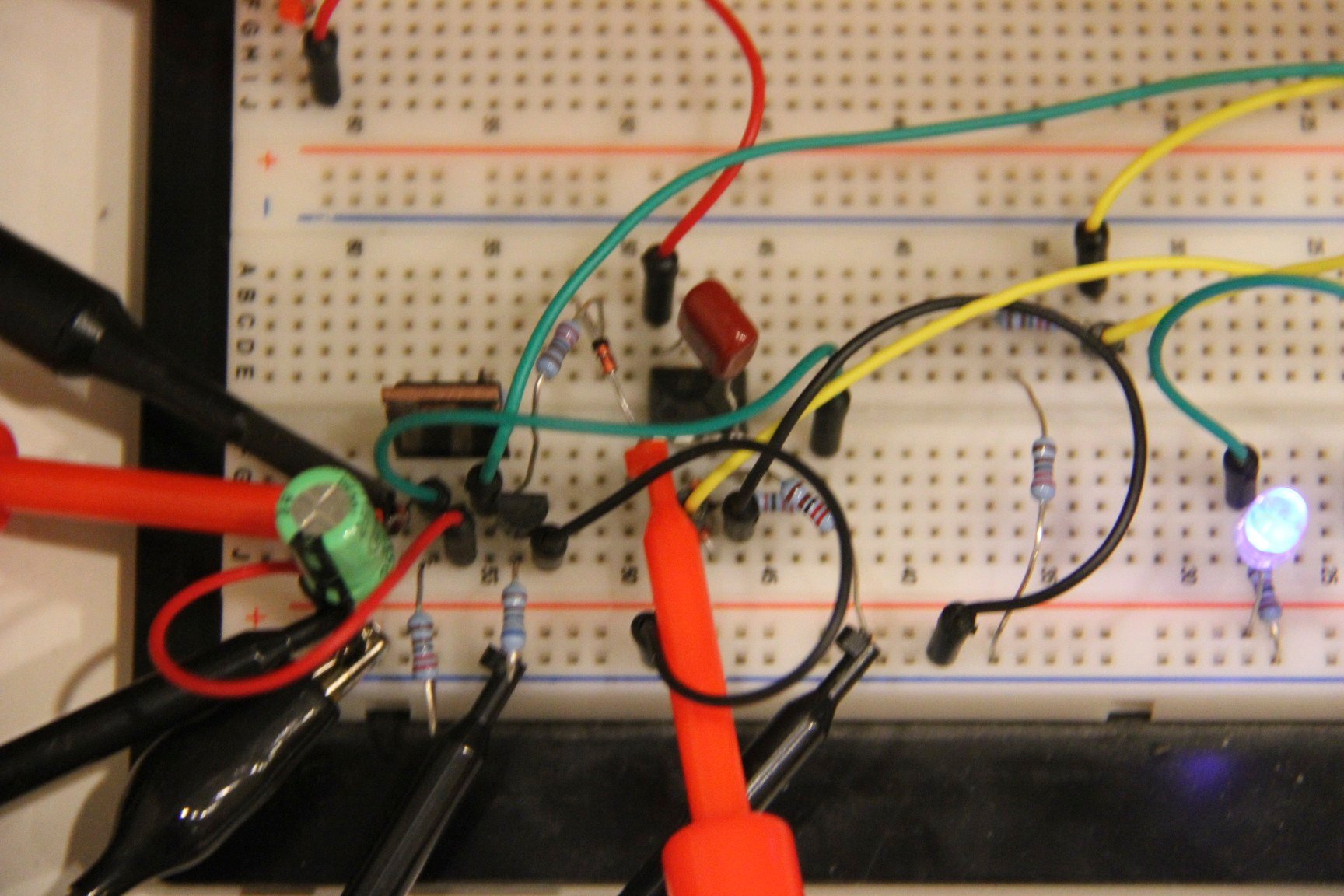
Now the overall high level system design and parameters are set (see Part 1), its time to get down to some practical design. As I specifically do not want to use one of those “out-of-the-box” all in one regulator chips the first thing we need is a working linear voltage regulator that we can build upon. Using the prototyping breadboard I created the following circuit. The objective was to set up and verify the DC conditions for a basic regulator. Unlike a classic regulator circuit where there is typically a fixed reference and a variable resistor (POT) in the feedback loop, this regulator calls for something slightly different because our micro controller and appropriate DAC will generate an accurate reference voltage between 0 and a couple of volts, the exact value of which will be set by the user; the regulator circuit must track this reference voltage and set its DC output to a multiple of that reference.
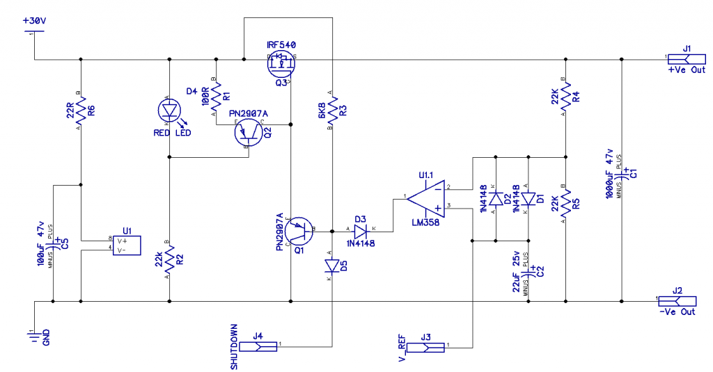
The following schematic shows my initial 30 minute attempt at building such a regulator.
I should state at this point that the circuit is basic and is missing lots of things that one would expect to find. The purpose of this initial design was not to create a perfect regulator but was to setup a circuit to verify the basic DC conditions and theoretical practicality of the circuit.
The circuit is built around a FET pass device (type IRF540) which is the power workhorse. Unregulated power into the drain with the load placed on the source. The op-amp is configured as a simple error amplifier. The op-amp will move its output up or down (depending on the input state) in order to get its two inputs as close together as possible. Because the op amp drives the power device and the negative input of the op-amp is derived from the output that the power device we have a closed loop servo circuit and this is in essence what a typical regulator is made up of.
Because of the closed loop nature and the tight feedback loop, one of the biggest problems with these types of control circuits is stability. Each component and any introduced capacitive or inductive loading will create phase shifts (all components exhibit parasitic capacitance and inductance). Phase shifts will put the circuit into positive feedback at certain frequencies so there is a good possibility that such a circuit will become an oscillator at certain frequencies. As a consequence, a great deal of attention needs to be paid to this problem in the design which needs to ensure that it works reliably and remains stable within the scope and specs of the requirements. The more voltage and current range required the more difficult it is to tune the circuit to be stable of the range. Component choice, DC conditions, speed/bandwidth, gain, noise and PCB/Track layout all matter a lot here. It’s for this reason that many power supply designs avoid discrete solutions in favour of a one-chip solution. Discrete regulators are hard to make, and even harder to make reliable and stable and to be honest, most people cannot be bothered when there is a $2 off the shelf IC that will do the job most of the time. However, a professional grade programmable bench power supply needs something more than what these one chip solutions offer.
Considering the breadboard approach to building the above circuit (see photo) under moderate loads the regulator circuit was pretty stable, actually I was very surprised just how stable it was.
I thought I was on my way but very quickly realised I was actually on the wrong track. The reason why this design is stable is because it does not have much gain, in fact it has a gain of just 2. So put 2 volts into the V_REF input and get 4 volts out. The driver transistor Q1 is in effect a current amplifier in this configuration – the op-amp has to swing its output pretty much the range of the desired output. For low voltage requirements where you con comfortably run your entire circuit from a single supply this is a very good approach because of the inherent stability of the circuit. However, this design requires a regulated output of 0-30v which would require the unregulated input voltage after the rectifier and reservoir caps to be about 45 Vdc. Not many op amps can run at this level, and those that can are only just within range so we would be right on the edge of the spec for the device which does not make for a robust design and I personally don’t like components being pushed to their limits – it feels wrong, a bit like driving your car continuously in the red like, you can do it but not many people want their car to scream like that all the time.
In order to facilitate ease of use and the modular design I have set out to achieve, I want to create a regulator module that runs from a single AC power source, a single winding from the mains transformer. Many bench PSU’s (for example, like the Agilent E3631A I recently repaired) have multiple internal power supplies where the control circuitry is powered separately from the main power source. This makes it easier to design for higher regulated voltages and helps with things like noise immunity too but because of the design goals I have set it’s not an option for this design.
The design needs to take into account some system design constraints. No split supply for the op-amps, so we need to use single-supply capable devices. The op-amps and control circuitry need to run at a much lower voltage than the pass device and regulator output and the only way that is possible is by introducing voltage gain outside of any op amp. Voltage gain using an emitter follower (or equivalent approach) provides the level translation needed and lots of gain but that’s where the stability problems start.
In Part 3 I will describe the next evolution of the regulator circuit where I introduce gain and a considerable amount of instability and start to formulate a workable solution.

