Fully Programmable Modular Bench Power Supply – Part 7

Now I have the requirements for the control ranges I need its time to get down to the nitty-gritty and get a DAC up and running so we can make some measurements. The maximum dynamic range I need for this project is 6000 individual steps – this was identified in the calculations for the voltage control for the 0-6V rage in Part 5, so let us start there.

There are many options for DAC’s to choose from, I want to keep the cost and component count down so my starting point is a low-cost single component solution from Microchip, part number MCP4822. This is a dual 12-bit DAC with two channels and a built-in voltage reference. I get independent voltage and current control from one 8-pin chip – wow! However, there is a problem with this part, it only has 12-bit resolution which will only give me 4096 individual steps and my design calls for 6000. The problem with choosing components with a higher number of bits is that they start to get expensive. I want to see if it’s possible to extend the range of the DAC using software and a technique called “dithering” or “modulation”.

The idea here is pretty simple, to increase the resolution of the DAC you can continuously switch the output between two or more codes, feed the result into a low-pass filter and get the average voltage. If you switch between two adjacent codes with a variable mark space ratio like you do in PWM, it should be possible to extend the range of the DAC without creating large ripples on the voltage head making the low pass filter easy to construct. That is the theory at least, I need to try it and see what the results are in practice.

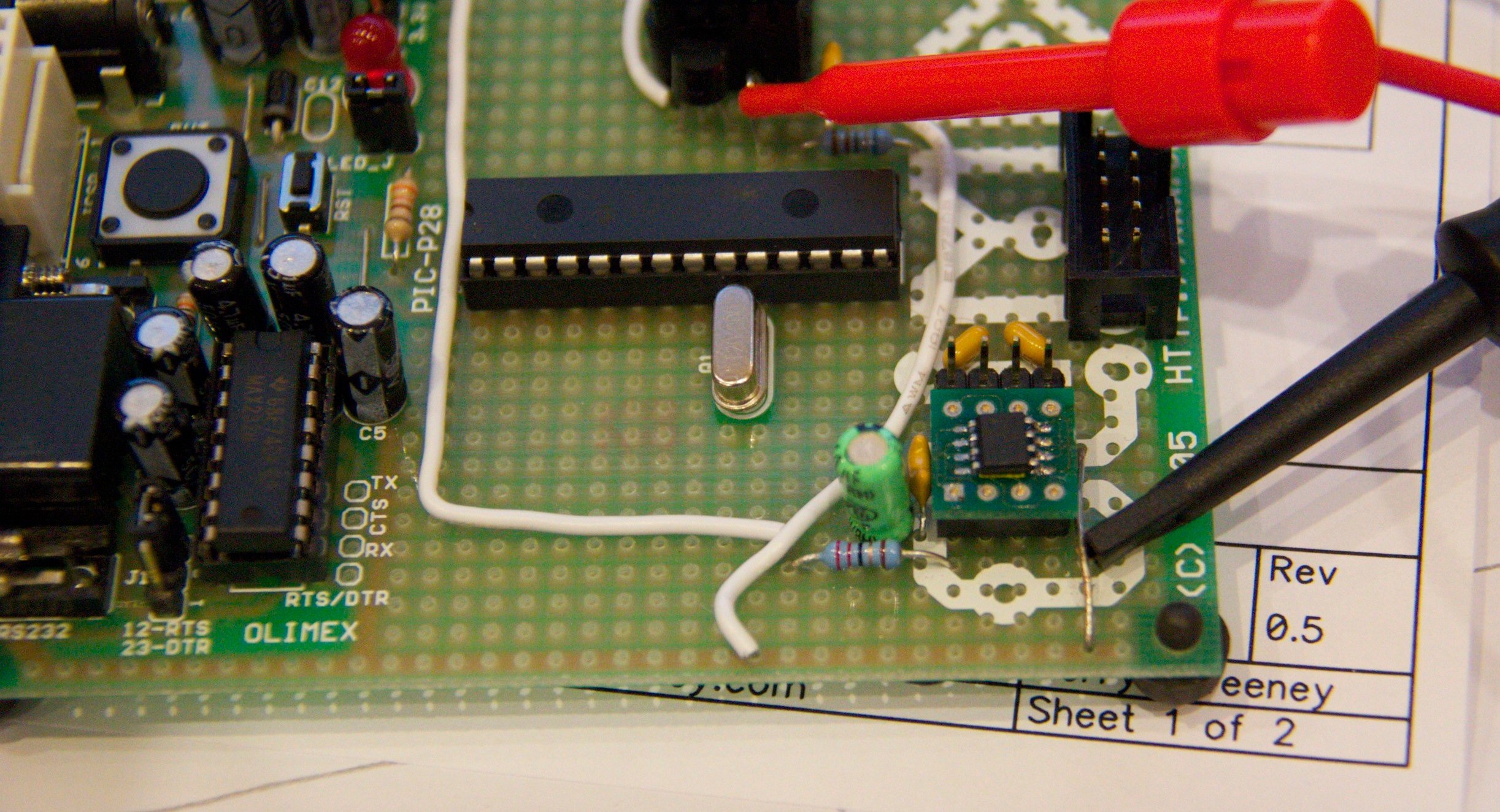
Before getting too complicated though, I thought it would be good to run the DAC in static mode, set some codes and measure what we get. The DAC has 4096 steps, the internal reference voltage is 2.048v and the chip has a x2 gain option so I should be able to program any voltage between 0v and 4.096v in 1mV steps by simply programming a digital code between 0 and 4096 into the DAC channel. To get this up and running I hooked up a PIC micro controller, the DAC chip and an RS232 serial interface. The firmware in the PIC will allow me to interact with the DAC through a simple serial terminal on my computer.

Before any MPS430, Atmel or Arduino die-hard fans start giving me advice on micro controller choice — forget it. They are all good parts, I just happen to personally like PIC’s because I know them and I have the tools and a whole bunch of them sitting here to play with – if you are not happy with my choice of micro controller thats tough…. I am not going to change it or enter into any debate over the pro’s and cons of other devices – I am sticking with PIC’s for this one and if you try to change my mind I will ignore you – sorry.

Here is the schematic diagram for the prototype I am using.
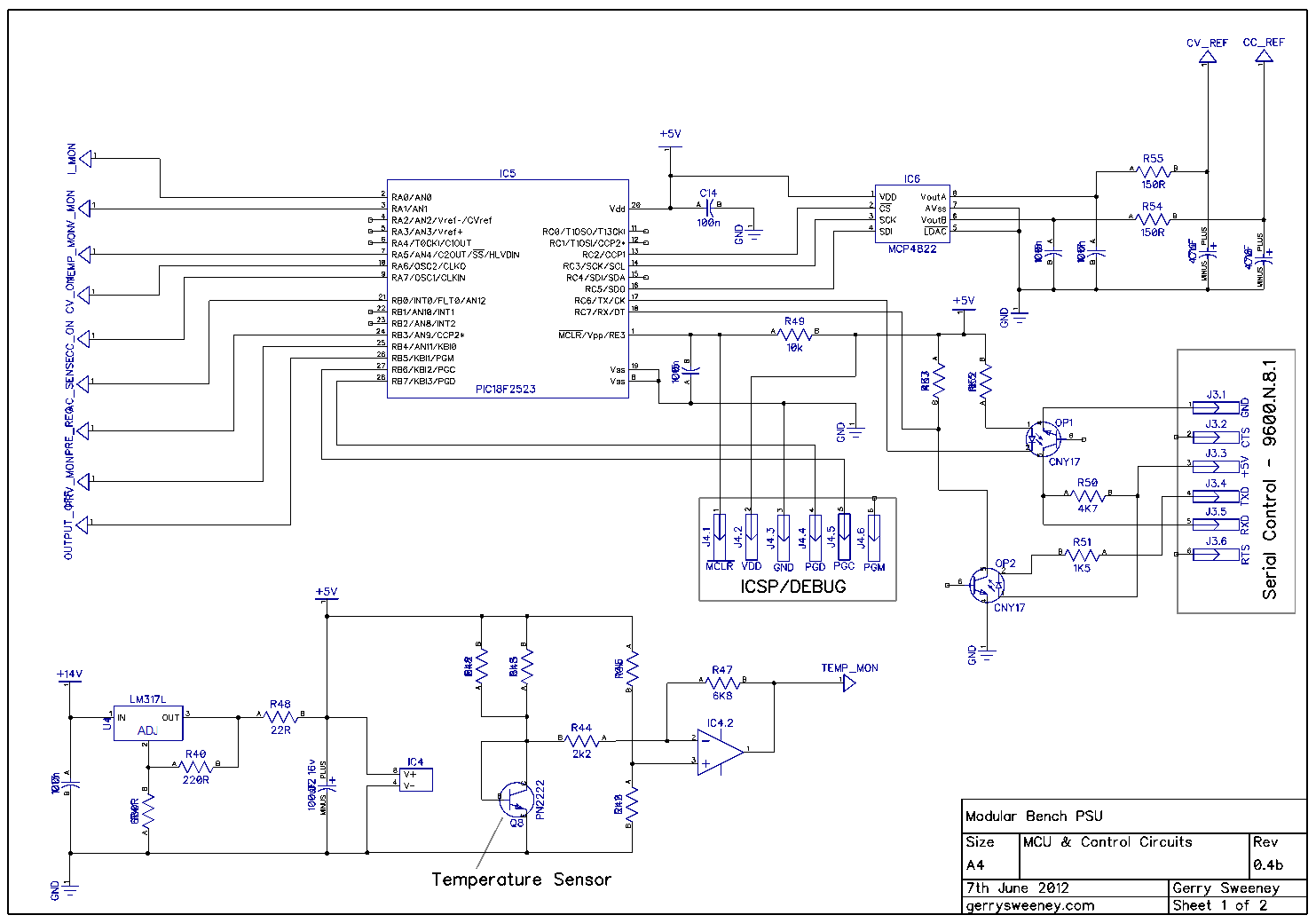
For the dithering I have decided to extend the DAC by 2 bits. Extending by two bits means I have to write a sequence of four codes continuously in succession to the DAC. I am writing approximately 1000 codes per second within a timer driven high-priority interrupt routine which ensures that the timing remains constant. Timing errors will introduce more DNL errors so the code stream needs to be constant and accurate. The codes written are the base code value followed by the base code value + 1. The two least significant bits from the now 14-bit word controls how many times each of the two values is written. For example, to get four steps between code 100 and code 101 we would write the following codes: –

100.00       100   100   100   100
100.25       100   100   100   101
100.5        100   100   101   101
100.75       100   101   101   101

Extending by 3 bits is an option and would mean I have to write a sequence of eight codes, again following the same explanation as above, here are the codes that would be written

100.00        100   100   100   100   100   100   100   100
100.125       100   100   100   100   100   100   100   101
100.250       100   100   100   100   100   100   101   101
100.375       100   100   100   100   100   101   101   101
100.500       100   100   100   100   101   101   101   101
100.625       100   100   100   101   101   101   101   101
100.750       100   100   101   101   101   101   101   101
100.875       100   101   101   101   101   101   101   101

I tried the three bits as an academic exercise but I have decided not to go to three bits because of the noise, ripple and integral errors generated. The cost of the filter circuitry and the expansion of the line items in the bill of materials would probably outweigh the cost of upgrading the DAC component to a higher resolution part.

I have selected a number of spot voltages in the range to benchmark what I get from the DAC. The following table sets out the results I measured. (I am using a calibrated HP 34401A meter for all measurements).

Spot Voltage DAC Code Measured
MCP4822
(12bit static)
Error DAC Code Measured
MCP4822
(14bit dith)
Error
0 0 0.0015V +0.0015V 0 0.0014V +0.0014V
0.001V 1 0.0015V +0.0015V 4 0.0016V +0.0002V
0.002V 2 0.0024V +0.0014V 8 0.0026V +0.0006V
0.003V 3 0.0034V +0.0004V 12 0.0036V +0.0006V
0.004V 4 0.0044V +0.0004V 16 0.0046V +0.0006V
100mv 100 0.1024V +0.0024V 400 0.1026V +0.0026V
500mv 500 0.5024v +0.0024 2000 0.5026V +0.0026V
501mv 501 0.5034v +0.0024 2004 0.5036V +0.0026V
1V 1000 1.0004V +0.0004V 4000 1.0006V +0.0006V
1.5V 1500 1.4975 -0.0025 6000 1.4977V -0.0023V
2.5V 2500 2.5014 +0.0014 10000 2.5016V +0.0016V
3V 3000 2.9993 -0.0007 12000 2.9995V -0.0005V
3.001V 3001 3.0002 +0.0002 12004 3.0005V +0.0005V
3.002V 3002 3.0012 -0.0008 12008 3.0014V +0.0006V
3.9v 3900 3.8968 -0.0032 15600 3.8969V -0.0031V
4.095v 4095 4.0916 -0.0034 16379 4.0916V -0.0034V

Well, that is disappointing given I am aiming for a precision of 1mV and to get a control voltage of 0-6V I need accurate 500µV steps. So whats wrong here? Having read the data sheet there are some gotcha’s that naively you might ignore as I did. Every DAC has two really important parameters called Integral Non-linearity (INL) and Differential Non-Linearity (DNL). The DNL defines the maximum deviation to expect from the “ideal” voltage for any given code, expressed in LSB’s (or counts from ideal) and INL is the accumulated DNL errors that occur over the whole range. Fundamentally, the DAC is based on a resistor string network and its not easy to make highly accurate resistors, as soon as you start needing more accuracy the cost of the part rises very steeply, and even with the best part money can buy there will still be errors. The more bits you extend the DAC by using dithering, the more error you introduce and the more noise you introduce too. While extending by two bits is probably acceptable with a decent low-pass filter, extending by three bits and beyond is not really practical. As an aside, the noise figures for the MCP4x22 parts are not that great – something one must consider when the reference voltage generated is going to be amplified, the noise will also be amplified.

In summary then, I want accuracy and precision but I want reasonable cost and even if I spend a lot of money I will still have errors. The lesson learned for me is I now no longer think of a DAC as an accurate programmable voltage source – it’s not, it is a close approximation only. The MCP4922 (MCP4822) is a nice part for the $$$ and useful for some things I have no doubt, but it’s not good enough for what I want to achieve in this project. Even with the resolution extension to 14-bits it falls short. Actually to be fair, even with the errors in the DAC this would be make a pretty good degree of control, it is probably more accurate than most of the lower end bench PSU’s out there, but my benchmark is the Agilent E3631A so I need to achieve much better than this. The MCP4x22 device is the best resolution DAC Microchip do so I must now search for other parts instead – Linear Technologies and Analog Devices are the logical starting point for my search.

There is one further possibility which I have yet to try, which is to combine both 12-bit DAC outputs to create a much higher resolution DAC, the block diagram for such a solution is shown in the data sheet for the part. This is well worth a look because if it works well enough, the cost of the two chips may well still be cheaper than an upgraded DAC part. I will build this out at some point and give it a try.

This project also needs to implement metering in order to monitor the output volts and current drawn by the load connected to the PSU, and this needs to be reasonably accurate to 1mV too, that’s 5-digits I need which in its self is a tall order. However, it occurred to me that if I could get an ADC that was accurate enough and a DAC with enough resolution to provide headroom for trimming it might be possible to build a self-calibrating system that trims the DAC output to match the desired programmed voltage each time you set a new voltage. That is what I will look at in Part 8.
Schematic and PCB Software – I Wish!

A long time frustration of mine has been the lack of good quality, easy to use electronic design software, I have tried a few and I am even a licensed user of the tool I consider to be the best of a bunch which is Diptrace (http://www.diptrace.com/), but its poor enough in some areas that even after buying a licence I am left with a burning desire to look for better options or as I have been sometimes known to do – write my own!

There are many packages available but all have their problems, usability, quality and intuitiveness are all lacking. Most of the packages are long-standing code bases that have been around for years and all appear dated in use. Packages are not interoperable and are based on proprietary file and library formats so once you are using one you are essentially tied in. You are also mainly limited to Windows with very limited support for Mac and Linux. The top of the range packages are outrageously expensive and closed off to the hobbyist/small business/one-man designer operations, this market is served by a number of budget systems, the best of which is still really only average. The more expensive solutions are packed full of features that are rarely used by most, Altium Designer (http://www.altium.com/) is one such tool and its users complain a lot about the lack of R&D dollars spent on the core functionality as they see it, instead Altium put their effort into other things like integrated FPGA design capability or integrated software development features – all a nice idea but not really desirable when its to the detriment of features on the core product capabilities that most people use on a daily basis (Disclaimer: this view of Altium is not my own, it’s what I have read/picked up from various forums when I was seriously considering buying a license for the tool).

I would love to see an affordable EDA tool that would serve both hobby/maker community as well as professional users. The ideal package would avoid needless bloat and complexity by specifically focusing only on the four main functional areas that actually help electronics engineers design, document and make electronic projects. I would like this tool to be fast, intuitive to use (I mean intuitive in terms of windows/mac UI users as opposed to making it work like 90’s AutoCAD) and works equally as well on Windows, Mac and Linux. The four key areas in order of importance in order of priority are: –

Component Library Manager & Content

At the heart of any good EDA tool lies a component library manager and a component library (actual content, not just a nice editor). Almost every tool out there suffers from poor quality library content or tools to make creating library content easy. Most tools require the users to build their own libraries and components despite there being a finite number of standard footprints and symbols. There is of course always a need to create other specific components which is not to be ignored but the most common component symbols, footprints and components should be provided in the library by default. Perhaps a nice-to-have but some kind of central on-line component library database that would allow community contribution and sharing of components really easily right from within the software its self should exist. I believe that in the absence of a decent library of components a not even a great tool is any good.

Component Editor

The ability to create components easily is critical, If it’s a common component it should be a simple matter of finding it on a global database and importing it into your local library. However, when the component is not available it must be a trivial matter to create a new one. Most components are simple block components represented on a schematic diagram as a rectangle with pins extending from any of its four sides. There are no vector graphics drawn in these components so they can easily be defined in data form rather than in graphic/plot form as many products from the 80/90’s seem to do. Creating such components should be really fast to do and require very little layout design, simple data entry and a bit of layout to finish up is all that should be needed. The other kind of component is a vector graphic component, for example a transistor or diode. The best way of thinking of these components is to imagine a block component described above with the relevant pins added and a vector graphic drawn inside the rectangle — and the rectangle outline being hidden. It would seem sensible to allow the import of standard scalable vector graphics (such as SVG files) rather than try to re-create a graphics design tool within the system which many other solutions do – but very badly. There are good, free tools that are infinitely better than anything that could be made and maintained so to reflect the desire not to bloat the system with features that are rarely used then just importing such graphics would be a better starting point.

Schematic Capture

All electronics projects/designs start with a schematic diagram. In my ideal package, the schematic editor would be the heart of the entire solution that would drive many of the design aspects – this is different to most other tools which would appear to put PCB board design at the heart of the solution – this I think is a historical thing. A schematic diagram is a drawing that shows how all of the electronic components in a project connect to each other electrically (not physically). A good schematic capture tool should be easy to use first and foremost and should support all of the key features like hierarchical and multi-sheet designs, in-schematic component pin re-organisation to suit schematic being designed, smooth interactive zooming, panning and publish-quality rendering and printing. Net list creation should be automatic and make sense to the user. A decent Bill of Materials (BOM) really ought to be generated from the design with no effort, and not just a stupid text file or excel spread sheet with limited information. Native elements of a schematic should be implemented as first class items, and not simply as another type of component which most packages seem to do. Most of all designing a schematic should be a pleasant activity, the presentation of the schematic should be beautiful, smooth graphics, good use of subtle colours and tones and different stroke wights to add character to the components and their visualisation; I say this because I am opposed to the blocky lines, and ugly component presentation that most packages seem to provide. Just like any other creative activity, electronic design is a form or art and must be nice to look at. There is absolutely no reason with today’s computing capability available to use why you cannot create better graphics in designer mode.

PCB Design

Many electronics projects lead to a PCB design. A PCB design tool should be easy to use and feature packed, most tools do this reasonably well because before fully integrated solutions were available PCB design tools were the primary focus. As a result most tools today have their roots in PCB design with schematic capture playing second fiddle. It’s not unheard of for people to use two different vendors packages, one for PCB design and the other for schematic capture. There are standard file interchange formats for net-lists which makes this possible. Easy and intuitive to use, smooth zooming, panning and track editing, easy access to layer controls and component placement/organisation are all key. Manual routing should be supported and made as easy as possible, despite autoroutermania there is still very much a need for manual layout/editing.

PCB Auto Routing

Slightly controversial I imagine is my thoughts on auto-routing, it would appear on the face of it that one could get significantly better and faster results with more powerful computers in a cluster. Auto routing could be done by uploading the PCB landmass and net list to a cloud based service that would carry out the actual routing retiring the route design back to the tool. Not sure how well this approach would be received, but I certainly like the idea of it.

2D Panel Design

Most other tools do not seem include this feature which is odd because after PCB design it’s very common to want to make basic panels with holes, cut-outs and shapes etc. There are many generic 2D packages out there but my feeling is there ought to be something that is specifically designed for electronics related designs such as front/back panels, chassis panels and flat parts etc. Like the component library a cut-out and shapes library here would be a fantastic productivity boost in creating panels.

Is this too much too ask? Is it a pipe dream? If you have a view/opinion I would love to hear it, please take the time to comment.

Fully Programmable Modular Bench Power Supply – Part 6

In Part 5 I talked about the target ranges that the PSU module should be able to support and expanded in detail on the voltage range calculations, and I said the next part would be looking at the DAC control circuitry. However, I really need to do the same exercise for current limit control in order to understand the required current control voltage range and resolution we need to ensure our DAC selection is appropriate for our current limit control too.

Current sensing starts with a “current shunt” which is simply a low value resistor in series with the load inside the power supply that will drop a small amount of voltage across it that is directly proportional to the current flowing through it. Selecting the right value is critical to ensure that your current sensing circuit operates in the correct range while making sure that the power dropped across the shunt resistor does not take the component outside of a reasonable thermal range, ideally you want your shunt resistor to run at ambient room temperature under the largest supported load. The PSU design calls for current handling of up to 5A. Just like in the DAC calculations we want to aim for nice round numbers so we pick a resistor value that is going to meet all of these requirements. In the design I have chosen a value of 0.1 ohms which if you do a simple OHMS LAW calculation “E = I / R” you will see that for a 0.1R resistor we get 500mV dropped across it when 5A of current is flowing. The amount of power dissipated in the shunt resistor at 5A can be determined by the formula “P = E x I” which works out to be 2.5W so we need to make sure that our chosen resistor is able to deal with that power and adequately dissipate the two and a half watts of heat generated.

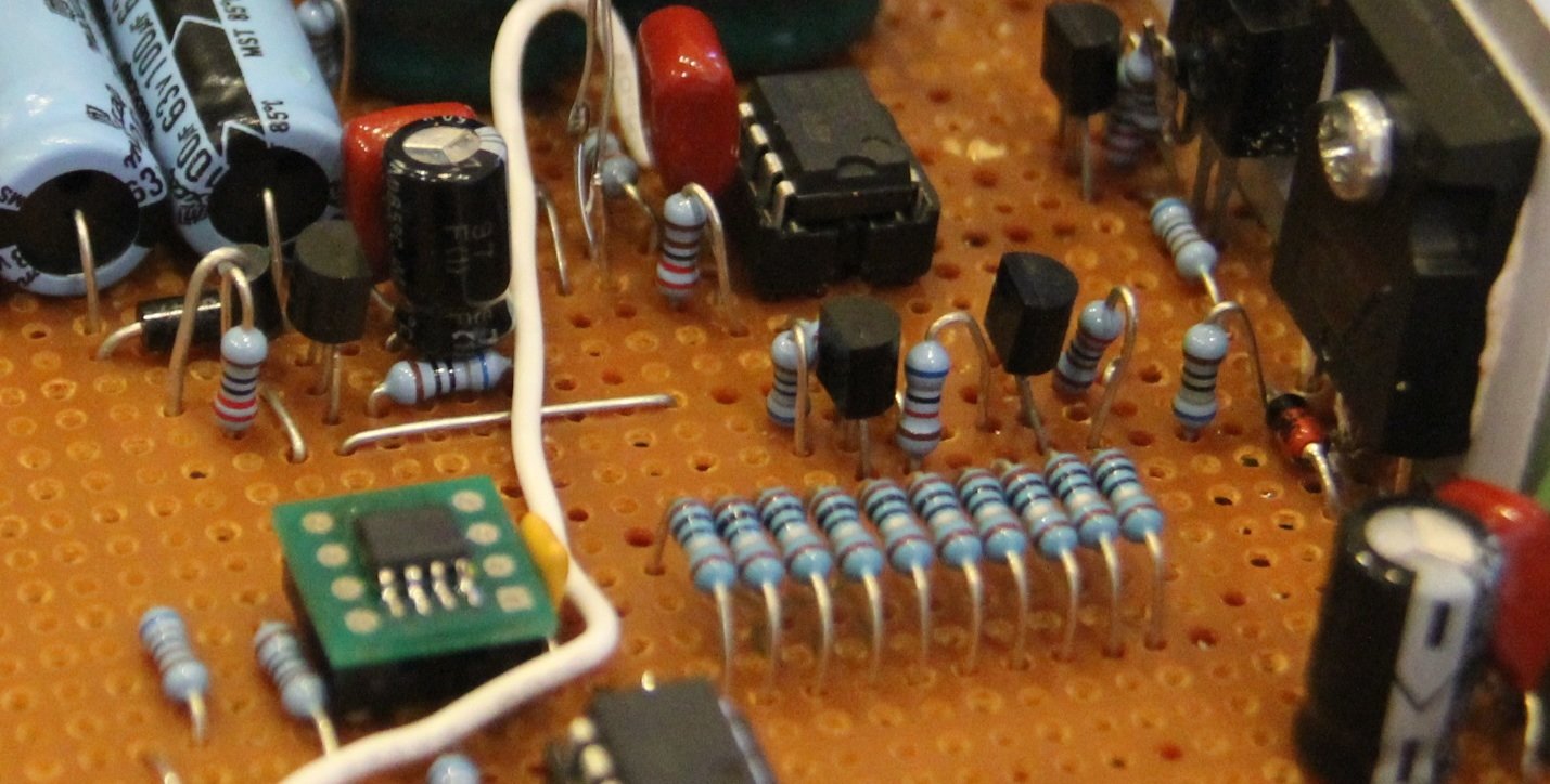
A 0.1R resistor is a common high-power resistor value, and for 5/10W resistors they are typically a wire wound construction. However, the tolerance on these resistors is around the 5-10% mark which we need to take into consideration. Just like the potential divider in the voltage sense circuitry, the current sense resistor is the only component in the circuitry that has a direct bearing on the accuracy of the the current sensing, so a 5% tolerance is really not good enough for what we want. Unfortunately, as soon as you need precision at low resistor values things start to get very expensive. Think about this, if you want a 0.1R resistor at 1% precision then our tolerance needs to be +/- 0.01 ohms which is very hard to make, hence the cost. I do wan’t the precision but without the cost, and am happy to be within 1% for the current sense, so a nice solution is to use 10 x 1R 1% 250mW resistors in parallel to create a 2.5w 0.1R 1% resistor. These resistors are cheap at just a couple of cents each and the tolerance will be tight enough that any error can be easily trimmed out in software calibration. The prototype I built uses through-hole parts that are soldered in but mounted about 5mm above the surface of the board providing airflow around them to help keep them cool. In production I may opt for using SMT resistors and a larger copper area to help dissipate the heat. Here is a photo of the construction described.

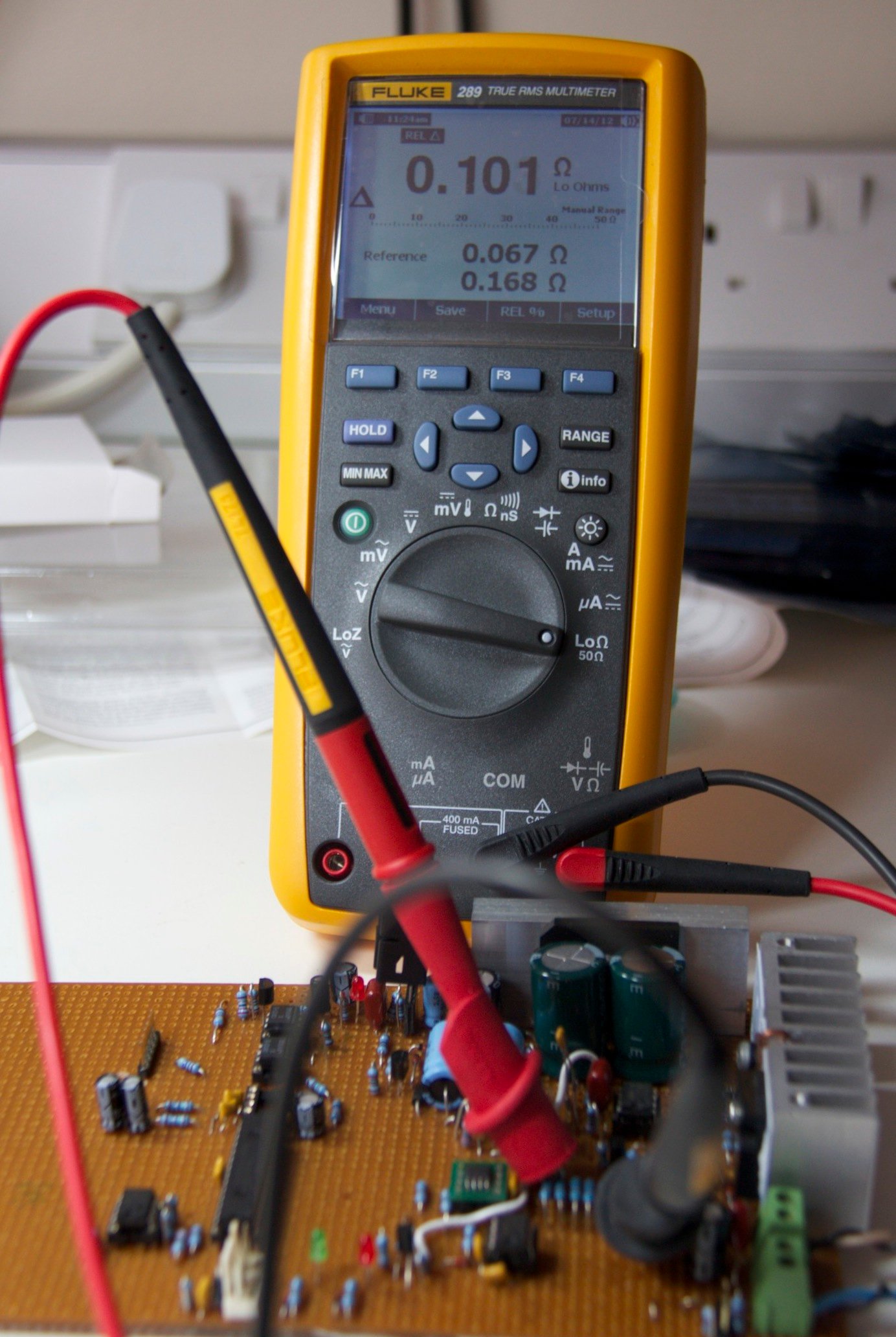
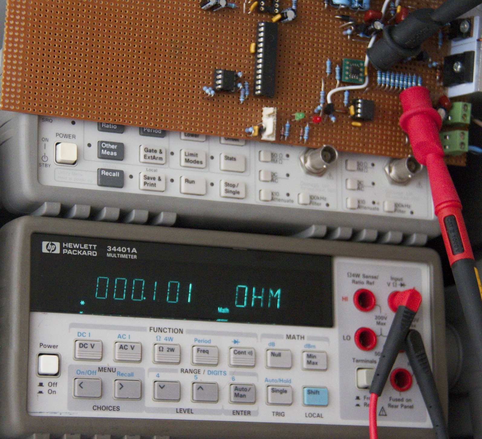
If accuracy beyond 1% is important you can hand pick resistors from different manufacturers batches and try to match the resultant restore created. If you fall slightly above the desired resistance you can trim it down by adding higher values in parallel. Or you can go down the “buy an expensive precision shunt resistor route”. In testing my own shunt though, I found I was within a few miliohms of 0.1R which is about what I would expect for 1% tolerance resistors. When measuring these resistances you need a meter that has a Relative or Null mode because you need to compensate for the meter leads and the mechanical contact. I used decent fluke leads and the supplied heavy duty croc clips, I used two different meters and nulled on the croc clips being shorted together before measuring the resistor. Here are the results…

Measured with a Fluke 289 on the low ohms range

Measured with a HP34401A on the ohms range

Now we know that our current sense resistor is good this will give us 0 to 500mV for 0-5A of current we need to sense that voltage and scale it up so we can do something useful with it. The MAX4080F I talked about in Part 4 does both of these things for us. This device is a purpose made high-side current sense amplifier and precision x5 gain amplifier with a buffered output. Being a high-side device its powered from the +V rail so we don’t need to do anything special. In our configuraiton and the x5 gain of the MAX4080F part we now have a buffered output voltage in the range of 0-2.5v for the current range of 0-5A. This control voltage is fed to the constant current error amp on the negative input creating a control loop that prevents the regulator from delivering any more current than is programmed. The current is set by applying the same voltage on the + input of the current error amp as the voltage that will be seen on the output of the MAX4080F device. If we provide a reference voltage of 500mV then the regulator will limit output current to 1A – Nice…

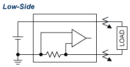
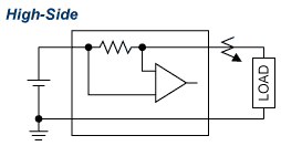
I thought it worth covering the two main schemes you can use to measure DC current in a power supply when using a current shunt resistor – these are known as high-side and low-side sensing.

        
NOTE: The above illustrations are from maxim-ic.com and are Copyright © 2012 Maxim Integrated Products

High side sensing is done on the hot regulated rail, often before the regulator pass device, whereas low-side sensing is done on the ground return path from the load. I have used high-side current sensing in this design because its the significantly better of the two schemes for a number of reasons, and its simple to implement because the MAX4080F makes it so. In the absence of such a useful single low cost purpose made device, then it could be tempting to go with low-side sensing because of simplicity. However, low-side current sensing designs introduce problems that our design will probably not tolerate. In low-side sensing the current sense resistor is placed in the load’s return path to ground, this has the undesirable effect of disturbing the common ground of the overall system when under load which can lead to stability problems, especially if we are doing remote sensing. Even worse than that is the risk that in a lab setup you are using a ground referenced PSU and in your test setup you ground your negative terminal of the PSU that has low-side current sensing which will effectively bypass or at the very least degrate the current sensing capability of your PSU which could cause a lot of damage, especially if your short circuit protection depends on the current sensing. Another problem with low-side sensing is as the current increases the ground reference and sense point will move apart as more voltage is dropped across the current sense resistor, this will introduce offset errors in voltage sensing. Low-side sensing is easy to do and easy to measure with a cheap op-amp but high-side current sensing brings so many advantages that $2 for the MAX4080F or another device like is money well spent I think.

One minor problem with the MAX4080F for this design is the common mode range of the device, the data sheet says it only goes down to 4.5V which is likely to be a problem in the case of a short circuit on the PSU output, really the common mode range needs to be able to extend to zero. I will need to test further to determine if it will be a problem in this design and possibly identify an alternative device – if anyone knows of any that are worth looking at please add a comment.

So back to the PSU, a quick recap on the ranges we are woking towards but this time with a focus on current sense and control.

Range Current
Range
Current Set
Resolution
Full Scale
Sense voltage
Volts per
Milliamp
Current
Steps
A 0-5A 1mA 2.5V 500µV 5000
B & C 0-2A 1mA 1V 500µV 2000
D 0-1A 1mA 500mV 500µV 1000

As you can see from the table above we have a more limited control range requirement so one configuration covers all ranges. However, there is a slight problem inasmuch as the design only gives us 2.5v out of the high-side amp at full scale, which is only 500µV per step which is half of what we get from our DAC at 1mV per step with a 4.096v reference. I can divide down the DAC output by x2 but then I fall short of the target range of 5A so I am going to have to rely on increasing the DAC’s resolution by modulating the DAC output – only measuring this physically will verify if thats good enough. Now we have a good sense of the control ranges need, in Part 7 I will work up a circuit, get a micro controller talking to the DAC chip and do some some perormance measurements to see what we come up with…. I know I said that in Part 5, but this time I mean it 🙂

Fully Programmable Modular Bench Power Supply – Part 5

I have set the regulator aside for a while, its time to turn to the control circuitry. However, before we get into the circuitry we need to do some pretty important calculations to help us select the right parts for the job. If you recall one of the aims for the power supply module is to be able to set its personality (supported voltage and current range) to suit a variety of voltage ranges. I have chosen a number of ranges to work within and specified them in the table below. Obviously its a relatively trivial task to add other ranges in the future so long as we stay within the confines of the working ranges of the components we have used in the system.

Range Volt
Range
Volt
Resolution
Volt
Steps
Current
Range
Current
Resolution
Current
Steps
Approximate
Power
Regulator
Gain
A 0-6v 1mV 6000 0-5A 1mA 5000 30W x2
B 0-16V 5mV 3200 0-2A 1mA 2000 40W x5
C 0-20V 5mV 4000 0-2A 1mA 2000 40W x10
D 0-30V 10mV 3000 0-1A 1mA 1000 30W x10

The values in the table above are what we use to establish the correct control circuitry so they probably deserve a bit of explanation. The voltage and current range columns speak for themselves, they tell us what the expected programmable range of the regulator will be. The voltage and current resolution columns tell us the size of each step in the range, so for example in range “A” which has a resolution of 1mv/1mA we can program the output volts from 0V to 6V in 1mV steps, and for the current we can program the limit from 0A to 5A in 1mA steps. The volts and current steps columns tell us how many digital codes are needed to represent the desired output voltage and resolution.

Getting our Voltage under Control

In oder to get a digitally controlled voltage we need to use a DAC (Digital to Analog Converter). A DAC takes a digital “code” and translates this directly to a static voltage. However, DAC’s typically operate in the 3.3v to 5.5v range so to control higher voltage ranges we need to ensure that the regulator circuit has gain. This is achieved by simply dividing the measured output voltage using two precision resistors before feeding back into the error amplifier. The column called “Regulator Gain” shows the gain factor required for the specified voltage range. You will see in the Part 4 schematic the gain has been set to x10 by R4 and R5. It is also with noting that these two resistors are the only two components in the entire regulator circuit that have any impact on the accuracy of the programmed output. The effects of inaccuracies in the other components are automatically and fully compensated for by the DC Servo effect created by the control loop. It is critical that R4 and R5 are accurate (I am using 0.1% tolerance resistors) and also have good temperature stability.

Alright, get to the point, what about the DAC!

In order to select the right DAC resolution and voltage reference (more on that later) we need to establish the range and resolution of the required control voltage. This is important because we must include the gain of the regulator which in turns affects the resolution requirements of the DAC. The following table expands on this with a key values we need to consider.

Range Output
Range
Resolution Steps Regulator
Gain
Reference
Range
Reference
Resolution
A 0-6v 1mV 6000 x2 0-3v 500µV
B 0-16V 5mV 3200 x5 0-3.2v 1mV
C 0-20V 5mV 4000 x10 0-2V 500µV
D 0-30V 10mV 3000 x10 0-3V 1mV

We calculate the control voltage range by dividing the target voltage by the gain multiplier value. For example, on range A, in order to obtain an output voltage of 6V we need a control voltage of 3V, calculated as 6 ÷ 3 = 2. To work out the reference control voltage resolution required we simply take the maximum controlling reference voltage needed and divide it by the number of steps required, in this case its 500µV per step.

From the above table we can clearly see that we need a maximum of 6000 steps to cover all ranges, which requires a DAC resolution of at least 13-bits. That is really inconvenient because DAC’s increase in price as the bits go up and there is a very notable jump in price as you go above 12-bits. A potential solution to this problem is to increase the step size on the 0-6v range from 1mV to 2mV which would half the resolution but would bring me nicely into range for a 12-bit DAC but I did not want to do that, its not what I set out to do, I needed to maintain the target resolution of 1mV on the 6v range. Thinking about it some more I thought that I could probably increase the resolution of the DAC in software using a technique whereby the DAC output is continuously set to a series of values at high speed to create an average voltage that can sit between between steps, this is known as dithering or modulating the DAC output. The downside to doing this is you introduce a peak ripple which reflects the continuously changing voltage level. However, filtering this out a straightforward affair because the amplitude of the ripple created is actually very small, so as long as we have enough current drive from the DAC a simple second-order passive low-pass filter is all that should be needed. Something worth noting though – the amplitude of the ripple voltage as an overall percentage of the output voltage is not linear; at lower voltages the ripple constitutes a larger proportion of the overall signal and therefore introduces more error. In practice though this should still end up well within tolerance, and if not we can always put in a higher resolution DAC!

One final thing is we need to decide on a reference voltage to use. DAC’s require a reference voltage in order to provide an accurate output voltage. Think of a DAC as a programmable potentiometer where the output is the wiper, the reference voltage is strapped across the two outer pins and the code sets the position of the potentiometer. If we have a 12-bit DAC that gives us 4,096 steps so if we use a reference voltage of exactly 4.096V we will have a theoretical output of 0-4.096V in 1mV steps which are nice round numbers that make software easier to develop, so that’s what we will go for.

So in summary, we have a design plan, we have our calculations and we know we need at least a 12-bit DAC. I am going to start with a DAC from Microchip MCP4822 which is a dual 12-bit DAC, its low cost and seems a reasonable starting point to do some experimenting, it also has a built in 2.048v reference and a x2 amplifier giving us the 0-4.096v @ 1mV steps.

In Part 6 I will work up a circuit, get a micro controller talking to the DAC chip and do some some perormance measurements to see what we come up with.

Horizontal and Vertical flip transformations of a QGraphicsItem in Qt QGraphicsView

I have been reviewing and assessing Qt for a small software project. Having only spent a small amount of time with the development environment I have managed to create a small program that allows me to draw 2D graphics. I have been using C++ for many years and for GUI related work I have mostly used MFC. I like C++ for UI’s because it makes programs that are fast and responsive, I plan to post an article comparing .NET, Java and C++ for building desktop applications in the near future.

Back to the library evaluation, one of the things I needed to be able to do was to flip a vector graphic item either horizontally or vertically around its center axis, meaning after the flip the object should be in the exact same place on the world view as it was before the transformation. There are built in functions for doing rotations around a center point but not this specific function. The 2D graphics system in QGraphicsView/QGraphicsItem uses matrix transforms which are at best very complicated – you need a good understanding of mathematics and a lot of patience to be able to comprehend this staff – I needed to understand this: –

Matrix

WTF! – does this mean anything to you? No, me either, thank heavens for those bright folk that work this stuff out for us…. if you do need to know more about the maths behind this you check out this document: http://en.wikipedia.org/wiki/Transformation_matrix which from what I can tell gives you the explanations, but I have to confess I switched off very quickly.

Having read that document I wanted to give up – too hard – or I am too lazy, either way i got a beer from the fridge and got nowhere – but not being one to give up so easy I decided that instead of learning the maths I would go back to debugging and good old-fashioned trial and error! Actually the Qt library has done most of the hard work, the fact that I can achieve my goal with a little bit of debugging, trial and error is testimony to that.

I did search around for examples and while there were lots of questions about this, there would appear to be very little in the way of answers, perhaps I am just a maths luddite or maybe there are many more people that shy away from the maths involved and say nothing 🙂 In the end I came up with this which appears to work very well, and given there would not appear to be much information out there on this particular requirement, I thought I should make this example available. Having all the individual variables makes for easy debugging, you can see what’s going on. I also included a simple debug function for dumping the transform matrix data.

+1 for Qt – check it out http://qt.nokia.com/products/

Low-cost Temperature Measurement

As part of the Fully Programmable Modular Bench Power Supply project I needed to measure the temperature of the heat sink in order to provide some thermal protection. The aim is simple enough, monitor the temperature of the heat sink and if it gets too hot shut it down until the temperature returns to an acceptable level. As it turns out there is more to this than one might think.

Firstly I needed to decide on a sensing device. There are numerous options to choose from falling into three main categories of passive, active linear and active digital.

Passive devices like RTD’s and Thermister’s are available in all sorts of types and are basically resistors that change value with temperature. These devices need circuitry around them and can be complicated to use mainly because their rate of change is expressed as a percentage per degree which in practice means a very non-linear response curve to temperature change. For my needs this was too complicated, at best I would need some kind of signal conditioning, feed into the micro controlled ADC and a software map of temperature vs. voltage to get a reading.

Digital devices such at the Dallas DS1821 can be connected to a micro-controller or in the case of the DS1821 a 1-wire serial bus. The device can be queried and it will return information about the current temperature it is sensing. These are very nice all digital devices but carry the penalty of cost, they are not cheap, costing upwards of $2 a piece. Because of cost I decided not to pursue the use of these

Analog devices are solid state devices that provide a variable voltage out that directly relates to temperature being sensed and are basically linear. These devices are typically low cost, simple three pin devices with power in, ground and volts out. The following are good devices to look at: –

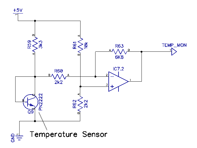
I was thinking about the Bill of Materials for my project and was not really wanting to add yet another part. I had read somewhere that silicone has a very linear temperature co-efficient of around -2mV/°C of temperature change, which means if you measure the voltage drop across a diode or transistor junction you will see a 2mv decrease in voltage dropped for every degree of temperature rise. As my circuit was already using some PN2222 devices which are general purpose NPN transistors and LM358‘s I thought it would be an interesting exercise to see if a simple discrete temperature sensor could be built.

Pen, paper, breadboard, some bits and an hour yielded the following circuit:

Temperature Sensor

This circuit provides a voltage swing of +1.5v to +3.5v for a temperature range of -50°C to +150°C. I was only able to test it down to a few degrees below zero but it tracked all the way up to 150°C without any problems. The data sheet for the PN2222 states it will operate down to -50°C so I have no doubt it will track downwards. Room temperature was at around 2v, I used a type K thermocouple and a Fluke 289 meter to calibrate it. The results of this circuit are surprisingly good and I did not add one single item to the BOM on the project, every component was already in use elsewhere in the circuit.

   
Average rating  1 2 3 4 5fYou must login to vote
IMG_5270.jpg
IMG_5275.jpg
IMG_5277.jpg
IMG_5283.jpg
IMG_5288.jpg
IMG_5292.jpg
IMG_5270.jpg
IMG_5275.jpg
IMG_5277.jpg
IMG_5283.jpg
IMG_5288.jpg
IMG_5292.jpg
IMG_5270.jpg
IMG_5275.jpg
IMG_5277.jpg
IMG_5283.jpg
IMG_5288.jpg
IMG_5292.jpg
 

Unfortunately the problem came when I needed to couple the device thermally. The main heat generating device on the project in question is an IRF540 in a TO-220 package. Bonding the PN2222 to the heat sink close to the device was my plan but in testing what I found was the lag between the IRF540 junction temperature and the heat skink temperature was enough that under extreme conditions the device will self-destruct long before the heat skink is hot enough to tell the control circuitry to shutdown. I found that the temperature on the plastic front of the device was much hotter than on the heat sink so I think the sensor really ought to somehow be mounted on the front of the device where the thermals are closer to the junction temperature than the heat sink. This exercise also convinced me to change the device to a bigger IRFP240 which is physically bigger and has better thermal properties. Although the data sheet for the IRF540 puts the device well within spec, I am more comfortable with the bigger package, more surface area must mean better thermal properties.

Back to the BOM – the PN2222’s that are in use in the project are in an SMT package so there was no practical way to thermally couple the two devices which meant I would need to add a TO-92 packaged device to the BOM and that really took away any advantage I had gained by using components already in the BOM for the project. I thought it still worth publishing the circuit as it may be of some use to others, pretty much any op amp and any silicon diode or transistor will yield much the same results.

In the end I opted to use the MCP9700A device from Microchip Technology, this is accurate enough for what I need and costs around $0.50 for a one-off. Still more expensive than the discrete design but I am trading that off for simplicity. The MCP9700A has a known temperature range and a known voltage output so interfacing to the MCU is as simple as connecting it to one of the ADC channels and measuring 10mV per degree of temperature – easy…..