A long time frustration of mine has been the lack of good quality, easy to use electronic design software, I have tried a few and I am even a licensed user of the tool I consider to be the best of a bunch which is Diptrace (http://www.diptrace.com/), but its poor enough in some areas that even after buying a licence I am left with a burning desire to look for better options or as I have been sometimes known to do – write my own!
There are many packages available but all have their problems, usability, quality and intuitiveness are all lacking. Most of the packages are long-standing code bases that have been around for years and all appear dated in use. Packages are not interoperable and are based on proprietary file and library formats so once you are using one you are essentially tied in. You are also mainly limited to Windows with very limited support for Mac and Linux. The top of the range packages are outrageously expensive and closed off to the hobbyist/small business/one-man designer operations, this market is served by a number of budget systems, the best of which is still really only average. The more expensive solutions are packed full of features that are rarely used by most, Altium Designer (http://www.altium.com/) is one such tool and its users complain a lot about the lack of R&D dollars spent on the core functionality as they see it, instead Altium put their effort into other things like integrated FPGA design capability or integrated software development features – all a nice idea but not really desirable when its to the detriment of features on the core product capabilities that most people use on a daily basis (Disclaimer: this view of Altium is not my own, it’s what I have read/picked up from various forums when I was seriously considering buying a license for the tool).
I would love to see an affordable EDA tool that would serve both hobby/maker community as well as professional users. The ideal package would avoid needless bloat and complexity by specifically focusing only on the four main functional areas that actually help electronics engineers design, document and make electronic projects. I would like this tool to be fast, intuitive to use (I mean intuitive in terms of windows/mac UI users as opposed to making it work like 90’s AutoCAD) and works equally as well on Windows, Mac and Linux. The four key areas in order of importance in order of priority are: –
Component Library Manager & Content
At the heart of any good EDA tool lies a component library manager and a component library (actual content, not just a nice editor). Almost every tool out there suffers from poor quality library content or tools to make creating library content easy. Most tools require the users to build their own libraries and components despite there being a finite number of standard footprints and symbols. There is of course always a need to create other specific components which is not to be ignored but the most common component symbols, footprints and components should be provided in the library by default. Perhaps a nice-to-have but some kind of central on-line component library database that would allow community contribution and sharing of components really easily right from within the software its self should exist. I believe that in the absence of a decent library of components a not even a great tool is any good.
Component Editor
The ability to create components easily is critical, If it’s a common component it should be a simple matter of finding it on a global database and importing it into your local library. However, when the component is not available it must be a trivial matter to create a new one. Most components are simple block components represented on a schematic diagram as a rectangle with pins extending from any of its four sides. There are no vector graphics drawn in these components so they can easily be defined in data form rather than in graphic/plot form as many products from the 80/90’s seem to do. Creating such components should be really fast to do and require very little layout design, simple data entry and a bit of layout to finish up is all that should be needed. The other kind of component is a vector graphic component, for example a transistor or diode. The best way of thinking of these components is to imagine a block component described above with the relevant pins added and a vector graphic drawn inside the rectangle — and the rectangle outline being hidden. It would seem sensible to allow the import of standard scalable vector graphics (such as SVG files) rather than try to re-create a graphics design tool within the system which many other solutions do – but very badly. There are good, free tools that are infinitely better than anything that could be made and maintained so to reflect the desire not to bloat the system with features that are rarely used then just importing such graphics would be a better starting point.
Schematic Capture
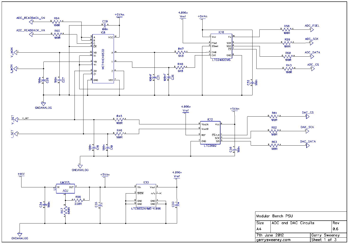
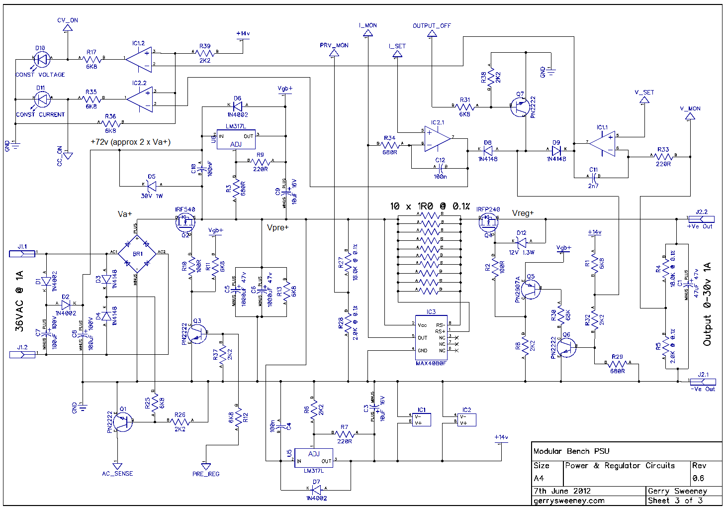
All electronics projects/designs start with a schematic diagram. In my ideal package, the schematic editor would be the heart of the entire solution that would drive many of the design aspects – this is different to most other tools which would appear to put PCB board design at the heart of the solution – this I think is a historical thing. A schematic diagram is a drawing that shows how all of the electronic components in a project connect to each other electrically (not physically). A good schematic capture tool should be easy to use first and foremost and should support all of the key features like hierarchical and multi-sheet designs, in-schematic component pin re-organisation to suit schematic being designed, smooth interactive zooming, panning and publish-quality rendering and printing. Net list creation should be automatic and make sense to the user. A decent Bill of Materials (BOM) really ought to be generated from the design with no effort, and not just a stupid text file or excel spread sheet with limited information. Native elements of a schematic should be implemented as first class items, and not simply as another type of component which most packages seem to do. Most of all designing a schematic should be a pleasant activity, the presentation of the schematic should be beautiful, smooth graphics, good use of subtle colours and tones and different stroke wights to add character to the components and their visualisation; I say this because I am opposed to the blocky lines, and ugly component presentation that most packages seem to provide. Just like any other creative activity, electronic design is a form or art and must be nice to look at. There is absolutely no reason with today’s computing capability available to use why you cannot create better graphics in designer mode.
PCB Design
Many electronics projects lead to a PCB design. A PCB design tool should be easy to use and feature packed, most tools do this reasonably well because before fully integrated solutions were available PCB design tools were the primary focus. As a result most tools today have their roots in PCB design with schematic capture playing second fiddle. It’s not unheard of for people to use two different vendors packages, one for PCB design and the other for schematic capture. There are standard file interchange formats for net-lists which makes this possible. Easy and intuitive to use, smooth zooming, panning and track editing, easy access to layer controls and component placement/organisation are all key. Manual routing should be supported and made as easy as possible, despite autoroutermania there is still very much a need for manual layout/editing.
PCB Auto Routing
Slightly controversial I imagine is my thoughts on auto-routing, it would appear on the face of it that one could get significantly better and faster results with more powerful computers in a cluster. Auto routing could be done by uploading the PCB landmass and net list to a cloud based service that would carry out the actual routing retiring the route design back to the tool. Not sure how well this approach would be received, but I certainly like the idea of it.
2D Panel Design
Most other tools do not seem include this feature which is odd because after PCB design it’s very common to want to make basic panels with holes, cut-outs and shapes etc. There are many generic 2D packages out there but my feeling is there ought to be something that is specifically designed for electronics related designs such as front/back panels, chassis panels and flat parts etc. Like the component library a cut-out and shapes library here would be a fantastic productivity boost in creating panels.
Is this too much too ask? Is it a pipe dream? If you have a view/opinion I would love to hear it, please take the time to comment.
